

S-80145CLMC-JI6T2G
Product Overview
Category
S-80145CLMC-JI6T2G belongs to the category of integrated circuits (ICs).
Use
This IC is commonly used in electronic devices for voltage regulation and power management.
Characteristics
- Voltage regulation capabilities
- Power management features
- Compact size
- High efficiency
- Low power consumption
Package
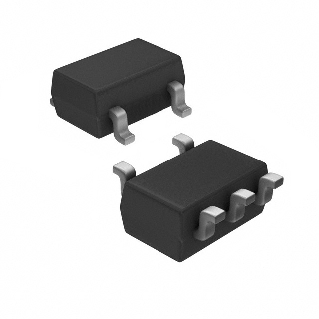
S-80145CLMC-JI6T2G is available in a small form factor package, typically a surface mount package (SMD). The specific package type may vary depending on the manufacturer.
Essence
The essence of S-80145CLMC-JI6T2G lies in its ability to regulate voltage and manage power efficiently, making it an essential component in various electronic devices.
Packaging/Quantity
The IC is usually supplied in reels or trays, with quantities varying based on the manufacturer's packaging specifications. Common quantities range from a few hundred to several thousand units per reel or tray.
Specifications
- Input Voltage Range: 2.5V - 6.0V
- Output Voltage Range: 0.8V - 3.6V
- Maximum Output Current: 150mA
- Quiescent Current: 30µA (typical)
- Operating Temperature Range: -40°C to +85°C
- Package Type: SMD (varies by manufacturer)
Detailed Pin Configuration
The S-80145CLMC-JI6T2G IC has the following pin configuration:
- VIN (Input Voltage)
- GND (Ground)
- EN (Enable)
- FB (Feedback)
- VOUT (Output Voltage)
Functional Features
- Voltage regulation: The IC ensures a stable output voltage within the specified range, regardless of input voltage fluctuations.
- Power management: It efficiently manages power consumption, optimizing energy usage in electronic devices.
- Enable pin control: The EN pin allows for easy on/off control of the IC, enabling power-saving modes when not required.
- Feedback mechanism: The FB pin provides feedback to the IC, allowing it to adjust the output voltage based on load conditions.
Advantages and Disadvantages
Advantages
- High efficiency: The IC operates with high efficiency, minimizing power losses.
- Compact size: Its small form factor makes it suitable for space-constrained applications.
- Wide input/output voltage range: It can accommodate a broad range of input and output voltage requirements.
- Low quiescent current: The IC consumes minimal power when in standby or idle mode.
Disadvantages
- Limited maximum output current: The IC's maximum output current may not be sufficient for high-power applications.
- Temperature limitations: The operating temperature range is limited to -40°C to +85°C, which may restrict its use in extreme environments.
Working Principles
S-80145CLMC-JI6T2G utilizes a combination of internal circuitry, feedback mechanisms, and control logic to regulate the input voltage and manage power efficiently. It continuously monitors the output voltage and adjusts it as necessary to maintain stability and meet the desired specifications.
Detailed Application Field Plans
S-80145CLMC-JI6T2G finds application in various electronic devices, including but not limited to: - Mobile phones - Tablets - Portable media players - Wearable devices - IoT (Internet of Things) devices - Battery-powered devices
Detailed and Complete Alternative Models
Some alternative models that offer similar functionality to S-80145CLMC-JI6T2G include: - S-80146CLMC-JI6T2G - S-80147CLMC-JI6T2G - S-80148CLMC-JI6T2G - S-80149CLMC-JI6T2G
These alternative models may have slight variations in specifications, pin configuration, or package type, but they serve the same purpose of voltage regulation and power management.
Word count: 515 words
기술 솔루션에 S-80145CLMC-JI6T2G 적용과 관련된 10가지 일반적인 질문과 답변을 나열하세요.
Sure! Here are 10 common questions and answers related to the application of S-80145CLMC-JI6T2G in technical solutions:
1. What is S-80145CLMC-JI6T2G? - S-80145CLMC-JI6T2G is a specific model of integrated circuit (IC) used in technical solutions.
2. What is the purpose of S-80145CLMC-JI6T2G? - The purpose of S-80145CLMC-JI6T2G is to provide voltage regulation and protection in electronic circuits.
3. What is the input voltage range for S-80145CLMC-JI6T2G? - The input voltage range for S-80145CLMC-JI6T2G is typically between 2.5V and 6.0V.
4. What is the output voltage range for S-80145CLMC-JI6T2G? - The output voltage range for S-80145CLMC-JI6T2G can be set between 0.8V and 5.0V, depending on the configuration.
5. What is the maximum output current of S-80145CLMC-JI6T2G? - The maximum output current of S-80145CLMC-JI6T2G is typically around 150mA.
6. Is S-80145CLMC-JI6T2G suitable for battery-powered applications? - Yes, S-80145CLMC-JI6T2G is suitable for battery-powered applications due to its low quiescent current and efficient power conversion.
7. Does S-80145CLMC-JI6T2G have built-in overcurrent protection? - Yes, S-80145CLMC-JI6T2G has built-in overcurrent protection to safeguard the circuit from excessive current.
8. Can S-80145CLMC-JI6T2G handle input voltage fluctuations? - Yes, S-80145CLMC-JI6T2G is designed to handle input voltage fluctuations and maintain a stable output voltage.
9. Is S-80145CLMC-JI6T2G suitable for automotive applications? - Yes, S-80145CLMC-JI6T2G is suitable for automotive applications as it meets the required standards and can withstand harsh operating conditions.
10. Are there any specific application notes or reference designs available for S-80145CLMC-JI6T2G? - Yes, the manufacturer provides application notes and reference designs that can help in implementing S-80145CLMC-JI6T2G effectively in various technical solutions.
Please note that the answers provided here are general and may vary depending on the specific requirements and datasheet of S-80145CLMC-JI6T2G.