

S-80859CNNB-B9KT2G
Product Overview
Category
S-80859CNNB-B9KT2G belongs to the category of integrated circuits (ICs).
Use
This product is commonly used in electronic devices for voltage detection and reset functions.
Characteristics
- Voltage detection range: 1.6V to 6.0V
- Low supply current: 1.0µA (typ.)
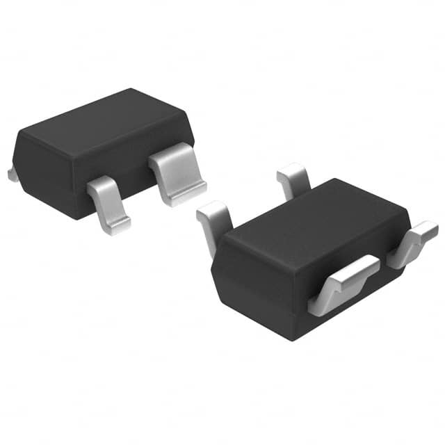
- Small package size: SOT-23-5
- Built-in delay circuit: 200ms (typ.)
Package
The S-80859CNNB-B9KT2G is packaged in a small outline transistor (SOT) package, specifically SOT-23-5. This package provides compactness and ease of integration into various electronic devices.
Essence
The essence of S-80859CNNB-B9KT2G lies in its ability to accurately detect voltage levels within a specified range and provide a reset signal when necessary. This feature ensures proper functioning and reliability of electronic systems.
Packaging/Quantity
The S-80859CNNB-B9KT2G is typically available in reels containing 3,000 units per reel.
Specifications
- Supply voltage range: 1.6V to 6.0V
- Operating temperature range: -40°C to +85°C
- Output type: Active low
- Quiescent current: 1.0µA (typ.)
- Reset threshold voltage options: 2.0V, 2.3V, 2.6V, 2.8V, 3.0V, 3.1V, 3.3V, 4.0V, 4.6V, 5.0V
Detailed Pin Configuration
The S-80859CNNB-B9KT2G has the following pin configuration:
- VDD: Supply voltage input
- GND: Ground reference
- RESET: Active low reset output
- MR: Manual reset input
- VOUT: Voltage detection output
Functional Features
- Accurate voltage detection within a specified range
- Active low reset signal generation
- Built-in delay circuit to prevent false resets
- Low quiescent current for power efficiency
- Manual reset capability for system control
Advantages and Disadvantages
Advantages
- Wide voltage detection range allows compatibility with various electronic systems
- Small package size enables integration in space-constrained applications
- Low supply current minimizes power consumption
- Built-in delay circuit prevents false resets, enhancing system reliability
- Manual reset input provides flexibility in system control
Disadvantages
- Limited reset threshold voltage options may not cater to all voltage requirements
- SOT-23-5 package may be challenging for manual soldering or rework
Working Principles
The S-80859CNNB-B9KT2G operates by continuously monitoring the input voltage (VDD) and comparing it against the preset threshold voltage. When the voltage drops below the threshold, the reset output (RESET) is activated, indicating a low voltage condition. The built-in delay circuit ensures that momentary voltage fluctuations do not trigger false resets.
Detailed Application Field Plans
The S-80859CNNB-B9KT2G finds application in various electronic devices where accurate voltage detection and reset functionality are crucial. Some potential application fields include:
- Battery-powered devices: Ensures proper shutdown or system reset when battery voltage reaches critical levels.
- Microcontrollers and digital systems: Provides reliable reset signals during power-up or voltage drop situations.
- Industrial automation: Monitors power supply voltages to prevent damage or malfunction of sensitive equipment.
- Automotive electronics: Facilitates safe operation by detecting abnormal voltage conditions and initiating appropriate actions.
Detailed and Complete Alternative Models
- S-80859CNMC-B9KT2G: Similar to S-80859CNNB-B9KT2G, but with a different package (SOT-23-6).
- S-80859CNPF-B9KT2G: Offers additional features such as adjustable reset delay time.
- S-80859CNUP-B9KT2G: Provides a wider range of reset threshold voltage options.
These alternative models offer similar functionality to the S-80859CNNB-B9KT2G, catering to different application requirements and preferences.
In conclusion, the S-80859CNNB-B9KT2G is an integrated circuit designed for accurate voltage detection and reset functions in electronic devices. Its compact size, low power consumption, and built-in delay circuit make it suitable for various applications. While it has some limitations, alternative models are available to address specific needs.
기술 솔루션에 S-80859CNNB-B9KT2G 적용과 관련된 10가지 일반적인 질문과 답변을 나열하세요.
Sure! Here are 10 common questions and answers related to the application of S-80859CNNB-B9KT2G in technical solutions:
Q: What is S-80859CNNB-B9KT2G? A: S-80859CNNB-B9KT2G is a specific model of voltage regulator IC (integrated circuit) manufactured by a particular company.
Q: What is the purpose of S-80859CNNB-B9KT2G? A: The purpose of S-80859CNNB-B9KT2G is to regulate and stabilize the voltage supply in electronic circuits or systems.
Q: What are the key features of S-80859CNNB-B9KT2G? A: Some key features of S-80859CNNB-B9KT2G include low dropout voltage, high output voltage accuracy, and overcurrent protection.
Q: In which applications can S-80859CNNB-B9KT2G be used? A: S-80859CNNB-B9KT2G can be used in various applications such as power management in consumer electronics, industrial equipment, and automotive systems.
Q: How does S-80859CNNB-B9KT2G help in technical solutions? A: S-80859CNNB-B9KT2G helps in technical solutions by providing a stable and regulated voltage supply, ensuring proper functioning of electronic components.
Q: What is the input voltage range supported by S-80859CNNB-B9KT2G? A: The input voltage range supported by S-80859CNNB-B9KT2G is typically between 2.0V and 7.0V.
Q: What is the output voltage range provided by S-80859CNNB-B9KT2G? A: The output voltage range provided by S-80859CNNB-B9KT2G is typically between 1.0V and 5.5V.
Q: Does S-80859CNNB-B9KT2G have any built-in protection features? A: Yes, S-80859CNNB-B9KT2G has built-in overcurrent protection, which helps prevent damage to the IC and connected components in case of excessive current flow.
Q: Can S-80859CNNB-B9KT2G operate in high-temperature environments? A: Yes, S-80859CNNB-B9KT2G is designed to operate reliably in high-temperature environments, making it suitable for various industrial applications.
Q: Are there any specific design considerations when using S-80859CNNB-B9KT2G? A: Yes, some design considerations include proper heat dissipation, input/output capacitor selection, and adherence to the manufacturer's recommended operating conditions.
Please note that the answers provided here are general and may vary depending on the specific requirements and datasheet of S-80859CNNB-B9KT2G.