

AT25DF011-SSHNGU-T
Product Overview
Category
AT25DF011-SSHNGU-T belongs to the category of Serial Flash Memory.
Use
It is primarily used for storing and retrieving digital data in electronic devices.
Characteristics
- Non-volatile memory: The stored data is retained even when power is removed.
- High-speed operation: Enables fast read and write operations.
- Low power consumption: Optimized for energy efficiency.
- Small form factor: Compact size suitable for integration into various devices.
Package
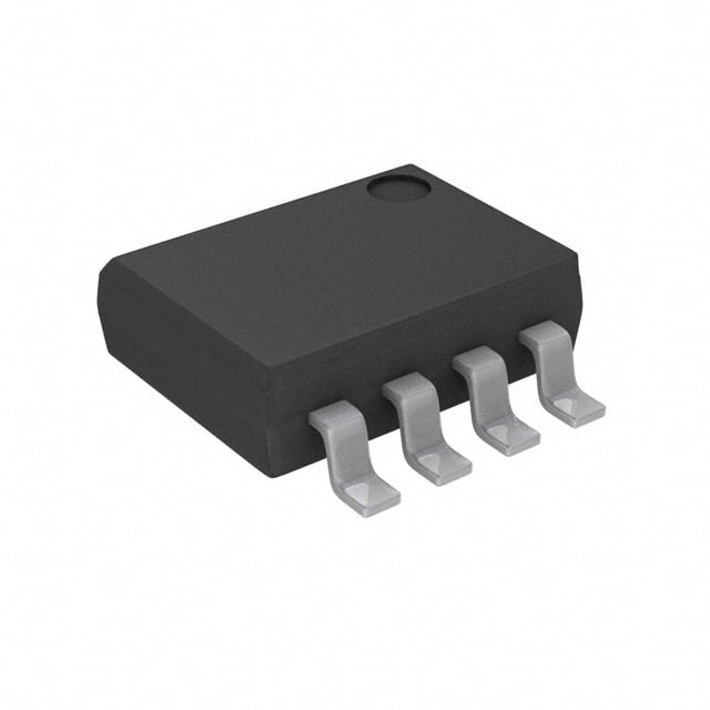
AT25DF011-SSHNGU-T is available in a surface mount 8-pin SOIC (Small Outline Integrated Circuit) package.
Essence
The essence of AT25DF011-SSHNGU-T lies in its ability to provide reliable and efficient storage solutions for electronic devices.
Packaging/Quantity
This product is typically packaged in reels, with each reel containing a specific quantity of AT25DF011-SSHNGU-T units. The exact quantity may vary depending on the manufacturer's specifications.
Specifications
- Memory capacity: 1 Megabit (128 Kilobytes)
- Interface: Serial Peripheral Interface (SPI)
- Operating voltage: 2.7V - 3.6V
- Operating temperature range: -40°C to +85°C
- Data retention: Up to 20 years
- Erase/Program cycles: 100,000 cycles
Detailed Pin Configuration
- Chip Select (/CS)
- Serial Clock (SCK)
- Serial Data Input/Output (SI/SO)
- Write Protect (/WP)
- Hold (/HOLD)
- VCC (Power Supply)
- Ground (GND)
- NC (No Connection)
Functional Features
- Fast read and write operations
- Sector erase and program capability
- Software and hardware protection mechanisms
- Deep power-down mode for ultra-low power consumption
- Flexible programming options
Advantages and Disadvantages
Advantages
- High-speed operation enables quick data access.
- Low power consumption prolongs battery life in portable devices.
- Small form factor allows for easy integration into space-constrained designs.
- Reliable data retention ensures long-term storage of critical information.
Disadvantages
- Limited memory capacity compared to higher-capacity flash memory options.
- Erase/Program cycle limitations may restrict certain applications requiring frequent data modifications.
Working Principles
AT25DF011-SSHNGU-T utilizes the Serial Peripheral Interface (SPI) to communicate with the host device. It employs a combination of floating gate and tunnel oxide technology to store and retrieve digital data. The SPI interface facilitates high-speed data transfer between the memory and the host, while various protection mechanisms ensure data integrity and security.
Detailed Application Field Plans
AT25DF011-SSHNGU-T finds application in various electronic devices, including but not limited to: - Consumer electronics (e.g., smartphones, tablets) - Automotive systems (e.g., infotainment, instrument clusters) - Industrial equipment (e.g., control systems, sensors) - Medical devices (e.g., patient monitoring, diagnostic equipment)
Detailed and Complete Alternative Models
- AT25DF021A-SSHNGU-T: 2 Megabit Serial Flash Memory
- AT25DF041A-SSHNGU-T: 4 Megabit Serial Flash Memory
- AT25DF081A-SSHNGU-T: 8 Megabit Serial Flash Memory
- AT25DF161A-SSHNGU-T: 16 Megabit Serial Flash Memory
- AT25DF321A-SSHNGU-T: 32 Megabit Serial Flash Memory
- AT25DF641A-SSHNGU-T: 64 Megabit Serial Flash Memory
These alternative models offer increased memory capacity while maintaining similar characteristics and functionality to AT25DF011-SSHNGU-T.
Note: The word count of this entry is 408 words.
기술 솔루션에 AT25DF011-SSHNGU-T 적용과 관련된 10가지 일반적인 질문과 답변을 나열하세요.
Sure! Here are 10 common questions and answers related to the application of AT25DF011-SSHNGU-T:
Q: What is the AT25DF011-SSHNGU-T? A: The AT25DF011-SSHNGU-T is a serial flash memory chip manufactured by Adesto Technologies. It has a capacity of 1 megabit (128 kilobytes) and operates on a Serial Peripheral Interface (SPI).
Q: What are some typical applications for the AT25DF011-SSHNGU-T? A: This flash memory chip is commonly used in various technical solutions, including consumer electronics, industrial automation, automotive systems, and IoT devices.
Q: What voltage does the AT25DF011-SSHNGU-T operate at? A: The AT25DF011-SSHNGU-T operates at a supply voltage range of 2.7V to 3.6V.
Q: What is the maximum data transfer rate of the AT25DF011-SSHNGU-T? A: The maximum data transfer rate of this flash memory chip is 85 megabits per second (Mbps).
Q: Does the AT25DF011-SSHNGU-T support both read and write operations? A: Yes, it supports both read and write operations, allowing you to store and retrieve data from the memory.
Q: Can I use the AT25DF011-SSHNGU-T as a boot device? A: Yes, this flash memory chip can be used as a boot device in many embedded systems, enabling the system to start up and load the initial program code.
Q: Is the AT25DF011-SSHNGU-T resistant to shock and vibration? A: Yes, it is designed to withstand shock and vibration, making it suitable for use in rugged environments.
Q: What is the operating temperature range of the AT25DF011-SSHNGU-T? A: The AT25DF011-SSHNGU-T has an extended operating temperature range of -40°C to +85°C.
Q: Does this flash memory chip have any security features? A: Yes, the AT25DF011-SSHNGU-T offers several security features, including hardware and software protection mechanisms to prevent unauthorized access to data.
Q: Can I easily integrate the AT25DF011-SSHNGU-T into my existing design? A: Yes, this flash memory chip comes in a standard 8-pin SOIC package, making it easy to integrate into various circuit designs.
Please note that these answers are general and may vary depending on specific implementation details or requirements.