

AS6C2008-55BIN
Product Overview
Category
AS6C2008-55BIN belongs to the category of semiconductor memory.
Use
It is primarily used for data storage in electronic devices such as computers, smartphones, and embedded systems.
Characteristics
- High-speed operation
- Low power consumption
- Non-volatile storage
- Large storage capacity
Package
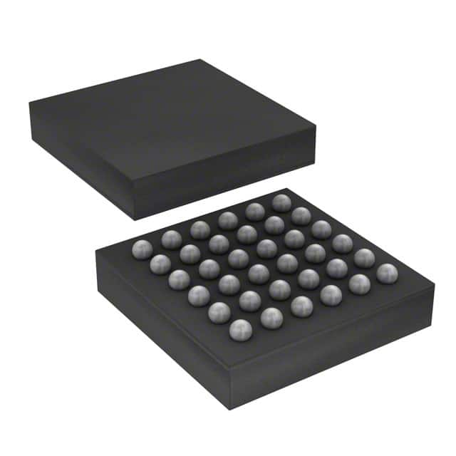
AS6C2008-55BIN comes in a compact package that is compatible with standard memory sockets.
Essence
The essence of AS6C2008-55BIN lies in its ability to store and retrieve digital information quickly and efficiently.
Packaging/Quantity
This product is typically packaged in trays or reels and is available in various quantities depending on customer requirements.
Specifications
- Memory Type: Static Random Access Memory (SRAM)
- Organization: 2 Megabit x 8-bit
- Operating Voltage: 3.3V
- Access Time: 55 nanoseconds
- Data Retention: More than 10 years
- Operating Temperature: -40°C to +85°C
Detailed Pin Configuration
AS6C2008-55BIN has a total of 28 pins, each serving a specific function. The pin configuration is as follows:
- Chip Enable (CE)
- Output Enable (OE)
- Write Enable (WE)
- Address Inputs (A0-A18)
- Data Inputs/Outputs (DQ0-DQ7)
- Power Supply (Vcc)
- Ground (GND)
Functional Features
- Fast read and write operations
- Easy interfacing with microcontrollers and other digital circuits
- Low standby current consumption
- Automatic power-down mode for further power savings
- Built-in error detection and correction mechanisms
Advantages and Disadvantages
Advantages
- High-speed operation allows for efficient data processing
- Low power consumption prolongs battery life in portable devices
- Non-volatile storage ensures data retention even during power loss
- Large storage capacity accommodates a wide range of applications
Disadvantages
- Relatively higher cost compared to other memory technologies
- Limited scalability beyond the specified storage capacity
- Susceptible to electromagnetic interference (EMI) and radiation-induced errors
Working Principles
AS6C2008-55BIN utilizes SRAM technology, which stores each bit of data in a flip-flop circuit. This allows for fast access times but requires constant power supply to retain data.
When a read operation is initiated, the addressed memory location is accessed and the stored data is retrieved. During a write operation, new data is written to the specified memory location.
Detailed Application Field Plans
AS6C2008-55BIN finds application in various electronic devices and systems, including: - Personal computers - Mobile phones - Networking equipment - Automotive electronics - Industrial control systems - Medical devices
Detailed and Complete Alternative Models
- AS6C4008-55BIN: 4 Megabit x 8-bit SRAM with similar specifications
- AS6C8008-55BIN: 8 Megabit x 8-bit SRAM with similar specifications
- AS6C16008-55BIN: 16 Megabit x 8-bit SRAM with similar specifications
These alternative models offer increased storage capacity while maintaining compatibility with AS6C2008-55BIN in terms of pin configuration and functionality.
In conclusion, AS6C2008-55BIN is a high-speed, low-power SRAM that provides reliable data storage for a wide range of electronic devices. Its compact package, functional features, and compatibility with alternative models make it a versatile choice for various applications.
기술 솔루션에 AS6C2008-55BIN 적용과 관련된 10가지 일반적인 질문과 답변을 나열하세요.
Sure! Here are 10 common questions and answers related to the application of AS6C2008-55BIN in technical solutions:
Q: What is AS6C2008-55BIN? A: AS6C2008-55BIN is a specific model of SRAM (Static Random Access Memory) chip commonly used in various electronic devices.
Q: What is the capacity of AS6C2008-55BIN? A: AS6C2008-55BIN has a capacity of 2 megabits, which is equivalent to 256 kilobytes.
Q: What is the operating voltage range for AS6C2008-55BIN? A: The operating voltage range for AS6C2008-55BIN is typically between 4.5V and 5.5V.
Q: What is the access time of AS6C2008-55BIN? A: AS6C2008-55BIN has an access time of 55 nanoseconds, which determines how quickly data can be read from or written to the chip.
Q: Can AS6C2008-55BIN be used in battery-powered devices? A: Yes, AS6C2008-55BIN can be used in battery-powered devices as long as the operating voltage requirements are met.
Q: Is AS6C2008-55BIN compatible with microcontrollers? A: Yes, AS6C2008-55BIN is compatible with most microcontrollers that support SRAM interfacing.
Q: Can AS6C2008-55BIN be used in industrial applications? A: Yes, AS6C2008-55BIN is suitable for use in industrial applications due to its wide operating temperature range and reliability.
Q: Does AS6C2008-55BIN support multiple read/write operations simultaneously? A: No, AS6C2008-55BIN is a synchronous SRAM and does not support simultaneous read/write operations.
Q: Can AS6C2008-55BIN be used in high-speed data processing applications? A: Yes, AS6C2008-55BIN can be used in high-speed data processing applications due to its relatively fast access time.
Q: Are there any specific precautions to consider when using AS6C2008-55BIN? A: It is important to ensure proper power supply decoupling and signal integrity measures when using AS6C2008-55BIN to maintain reliable operation.
Please note that the answers provided here are general and may vary depending on the specific application and requirements.