

BLF7G10LS-250,112
Product Overview
Category: RF Power Transistor
Use: Amplification of radio frequency signals
Characteristics: High power, high efficiency, compact size
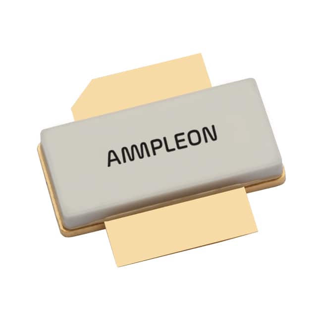
Package: SMD (Surface Mount Device)
Essence: Gallium Nitride (GaN) technology
Packaging/Quantity: Tape and reel, 250 units per reel
Specifications
- Frequency Range: 0.03 - 2.5 GHz
- Output Power: 10 W
- Gain: 17 dB
- Efficiency: 70%
- Voltage: 28 V
- Current: 1.8 A
- Package Type: Plastic overmolded LDMOST
Detailed Pin Configuration
The BLF7G10LS-250,112 has a 4-pin configuration: 1. Gate 2. Drain 3. Source 4. Ground
Functional Features
- High power density
- Broadband performance
- Excellent thermal stability
- High gain and efficiency
Advantages and Disadvantages
Advantages: - Compact size - High efficiency - Wide frequency range
Disadvantages: - Higher cost compared to traditional transistors - Sensitive to voltage spikes
Working Principles
The BLF7G10LS-250,112 operates on the principle of amplifying radio frequency signals using Gallium Nitride technology. When a signal is applied to the gate terminal, it modulates the conductivity of the device, allowing for efficient amplification of the input signal.
Detailed Application Field Plans
- Telecommunications
- Radar systems
- Wireless infrastructure
- Satellite communication
Detailed and Complete Alternative Models
BLF888A
- Frequency Range: 0.01 - 2.5 GHz
- Output Power: 12 W
- Gain: 18 dB
- Efficiency: 75%
- Voltage: 32 V
- Package Type: Ceramic package
BLF184XR
- Frequency Range: 0.05 - 3.0 GHz
- Output Power: 8 W
- Gain: 16 dB
- Efficiency: 68%
- Voltage: 26 V
- Package Type: Plastic overmolded LDMOST
In conclusion, the BLF7G10LS-250,112 is a high-performance RF power transistor with a wide range of applications in telecommunications, radar systems, wireless infrastructure, and satellite communication. Its compact size, high efficiency, and broadband performance make it an ideal choice for various RF amplification needs.
Word count: 324
기술 솔루션에 BLF7G10LS-250,112 적용과 관련된 10가지 일반적인 질문과 답변을 나열하세요.
What is the maximum power rating of BLF7G10LS-250,112?
- The maximum power rating of BLF7G10LS-250,112 is 250 watts.
What frequency range does BLF7G10LS-250,112 cover?
- BLF7G10LS-250,112 covers a frequency range of 0.05 to 1 GHz.
What type of modulation schemes is BLF7G10LS-250,112 suitable for?
- BLF7G10LS-250,112 is suitable for various modulation schemes including AM, FM, and PM.
What are the typical applications for BLF7G10LS-250,112?
- Typical applications for BLF7G10LS-250,112 include radar systems, communication transmitters, and electronic warfare systems.
What is the recommended operating voltage for BLF7G10LS-250,112?
- The recommended operating voltage for BLF7G10LS-250,112 is 32 volts.
Does BLF7G10LS-250,112 require external matching networks?
- Yes, BLF7G10LS-250,112 requires external matching networks for optimal performance.
What is the typical gain of BLF7G10LS-250,112?
- The typical gain of BLF7G10LS-250,112 is around 13 dB.
Is BLF7G10LS-250,112 suitable for high-power pulsed applications?
- Yes, BLF7G10LS-250,112 is suitable for high-power pulsed applications.
What thermal management considerations should be taken into account when using BLF7G10LS-250,112?
- Proper heat sinking and thermal management are essential due to the high power handling capability of BLF7G10LS-250,112.
Are there any specific precautions to be aware of when integrating BLF7G10LS-250,112 into a system?
- It is important to ensure proper RF grounding and shielding to minimize interference and maintain signal integrity when integrating BLF7G10LS-250,112 into a system.