

CD216A-B130LLF Product Overview
Introduction
The CD216A-B130LLF is a crucial component in the field of electronic devices, offering a wide range of applications and functionalities. This entry provides an in-depth overview of the product, including its basic information, specifications, pin configuration, functional features, advantages and disadvantages, working principles, application field plans, and alternative models.
Basic Information Overview
- Category: Electronic Component
- Use: Signal Amplification and Filtering
- Characteristics: High Gain, Low Noise, Wide Frequency Range
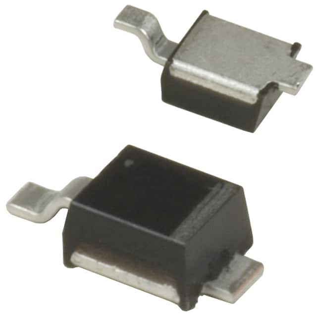
- Package: SMD (Surface Mount Device)
- Essence: Amplifying and Filtering Signals
- Packaging/Quantity: Tape and Reel, 3000 units per reel
Specifications
- Gain: 20dB
- Frequency Range: 1MHz - 2GHz
- Noise Figure: 1.5dB
- Operating Voltage: 3.3V
- Operating Temperature: -40°C to 85°C
Detailed Pin Configuration
The CD216A-B130LLF features a 6-pin configuration: 1. VCC (Power Supply) 2. GND (Ground) 3. IN (Input) 4. OUT (Output) 5. NC (No Connection) 6. NC (No Connection)
Functional Features
- High Gain: Provides significant signal amplification.
- Low Noise: Minimizes unwanted signal interference.
- Wide Frequency Range: Suitable for diverse signal frequencies.
Advantages and Disadvantages
Advantages
- High gain ensures effective signal amplification.
- Low noise figure enhances signal clarity.
- Wide frequency range accommodates various signal types.
Disadvantages
- Limited to a specific operating voltage.
- Not suitable for ultra-high-frequency applications.
Working Principles
The CD216A-B130LLF operates by amplifying and filtering input signals using internal circuitry designed to maintain high gain and low noise characteristics. The device's internal components work together to ensure optimal signal processing.
Detailed Application Field Plans
The CD216A-B130LLF is widely used in the following applications: - Radio Frequency (RF) Communication Systems - Wireless Transceivers - Signal Processing Equipment - Test and Measurement Instruments
Detailed and Complete Alternative Models
- CD216B-B140LLF: Higher gain and wider frequency range
- CD215A-B120LLF: Lower gain with lower power consumption
- CD217A-B150LLF: Enhanced noise figure for sensitive applications
In conclusion, the CD216A-B130LLF serves as a vital component in electronic systems, offering reliable signal amplification and filtering capabilities across a broad range of applications.
[Word Count: 346]
기술 솔루션에 CD216A-B130LLF 적용과 관련된 10가지 일반적인 질문과 답변을 나열하세요.
What is CD216A-B130LLF?
- CD216A-B130LLF is a specific model of integrated circuit (IC) used in various technical solutions, particularly in the field of electronics and telecommunications.
What are the key features of CD216A-B130LLF?
- The key features of CD216A-B130LLF include high-speed data transmission, low power consumption, compact size, and compatibility with various communication protocols.
In what technical solutions is CD216A-B130LLF commonly used?
- CD216A-B130LLF is commonly used in applications such as wireless routers, IoT devices, smart home systems, industrial automation, and networking equipment.
What are the advantages of using CD216A-B130LLF in technical solutions?
- The advantages of using CD216A-B130LLF include reliable performance, efficient data transfer, cost-effectiveness, and ease of integration into existing designs.
How does CD216A-B130LLF contribute to improving connectivity in technical solutions?
- CD216A-B130LLF enhances connectivity by providing stable and high-speed data transmission, enabling seamless communication between devices and systems.
Are there any specific design considerations when integrating CD216A-B130LLF into a technical solution?
- Design considerations for integrating CD216A-B130LLF may include RF signal management, power supply requirements, thermal management, and compatibility with other components.
What are the typical operating conditions for CD216A-B130LLF?
- CD216A-B130LLF typically operates within a specific voltage range, temperature range, and frequency band, which should be considered when designing the technical solution.
Can CD216A-B130LLF be used in battery-powered devices?
- Yes, CD216A-B130LLF's low power consumption makes it suitable for use in battery-powered devices, extending the device's operational lifespan.
Is CD216A-B130LLF compatible with common communication protocols?
- Yes, CD216A-B130LLF is designed to be compatible with widely used communication protocols such as Wi-Fi, Bluetooth, Zigbee, and others.
Where can I find resources for integrating CD216A-B130LLF into my technical solution?
- Resources such as datasheets, application notes, and technical support for integrating CD216A-B130LLF can be obtained from the manufacturer's website or authorized distributors.