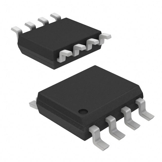
CY22801FXCT
Product Overview
Category
CY22801FXCT belongs to the category of programmable clock generators.
Use
This product is used for generating clock signals in various electronic devices and systems.
Characteristics
- Programmable clock frequency
- Low jitter
- Wide operating voltage range
- Small package size
- High reliability
Package
CY22801FXCT is available in a small form factor package, suitable for surface mount technology (SMT) applications.
Essence
The essence of CY22801FXCT lies in its ability to generate precise clock signals with programmable frequencies, catering to the specific requirements of different electronic systems.
Packaging/Quantity
CY22801FXCT is typically packaged in reels or trays, containing a specified quantity of units per package.
Specifications
- Input Voltage Range: 2.7V - 3.6V
- Output Frequency Range: 1MHz - 200MHz
- Output Format: LVCMOS
- Operating Temperature Range: -40°C to +85°C
- Supply Current: 10mA (typical)
Detailed Pin Configuration
CY22801FXCT has the following pin configuration:
- VDD: Power supply input
- GND: Ground reference
- XIN: Crystal oscillator input
- XOUT: Crystal oscillator output
- CLKOUT: Clock output
- SDA: Serial data input/output
- SCL: Serial clock input
Functional Features
- Programmable frequency selection
- Spread spectrum modulation support
- I2C interface for easy configuration
- Power-down mode for reduced power consumption
- Output enable/disable control
Advantages and Disadvantages
Advantages
- High flexibility due to programmable frequency selection
- Low jitter ensures accurate timing in electronic systems
- Compact package size allows for space-efficient designs
- Wide operating voltage range enables compatibility with various power supply systems
Disadvantages
- Limited output frequency range compared to some other clock generators in the market
- Requires external crystal oscillator for operation
Working Principles
CY22801FXCT utilizes a phase-locked loop (PLL) architecture to generate clock signals. The input frequency is multiplied and divided by programmable factors to achieve the desired output frequency. The PLL circuitry ensures stable and accurate clock generation.
Detailed Application Field Plans
CY22801FXCT finds applications in various electronic systems, including but not limited to: - Communication equipment - Consumer electronics - Industrial automation - Automotive electronics - Medical devices
Alternative Models
Some alternative models that offer similar functionality to CY22801FXCT include: - CY22800FXCT - CY22802FXCT - CY22803FXCT - CY22804FXCT
These models provide comparable features and can be considered as alternatives based on specific application requirements.
In conclusion, CY22801FXCT is a programmable clock generator that offers flexibility, accuracy, and reliability in generating clock signals for a wide range of electronic systems. Its compact size and wide operating voltage range make it suitable for diverse applications across various industries.
기술 솔루션에 CY22801FXCT 적용과 관련된 10가지 일반적인 질문과 답변을 나열하세요.
Sure! Here are 10 common questions and answers related to the application of CY22801FXCT in technical solutions:
1. What is CY22801FXCT? CY22801FXCT is a programmable clock generator IC that provides multiple clock outputs with low jitter and high accuracy.
2. What are the key features of CY22801FXCT? Some key features of CY22801FXCT include programmable frequency synthesis, low jitter performance, wide frequency range, and multiple clock outputs.
3. What is the operating voltage range for CY22801FXCT? CY22801FXCT operates within a voltage range of 2.7V to 3.6V.
4. How many clock outputs does CY22801FXCT provide? CY22801FXCT provides up to four clock outputs.
5. Can I program the output frequencies of CY22801FXCT? Yes, CY22801FXCT allows you to program the output frequencies through its configuration registers.
6. What is the typical jitter performance of CY22801FXCT? CY22801FXCT offers low jitter performance, typically below 200 femtoseconds (fs).
7. Can CY22801FXCT be used in high-speed communication systems? Yes, CY22801FXCT can be used in high-speed communication systems as it supports a wide frequency range and low jitter performance.
8. Does CY22801FXCT have any built-in fail-safe features? Yes, CY22801FXCT includes built-in fail-safe features such as power-on reset and glitch-free clock switching.
9. Is CY22801FXCT suitable for battery-powered applications? Yes, CY22801FXCT is suitable for battery-powered applications as it operates within a low voltage range and has low power consumption.
10. Are there any evaluation boards or development kits available for CY22801FXCT? Yes, Cypress Semiconductor provides evaluation boards and development kits for CY22801FXCT to facilitate easy prototyping and testing.
Please note that the answers provided here are general and may vary depending on the specific requirements and application scenarios.


