

제품 세부사항은 사양을 확인하세요.
CY7B9334-270JXC
Product Overview
Category
CY7B9334-270JXC belongs to the category of integrated circuits (ICs).
Use
This product is commonly used in electronic devices for signal processing and data transmission.
Characteristics
- High-speed performance
- Low power consumption
- Compact size
- Reliable operation
Package
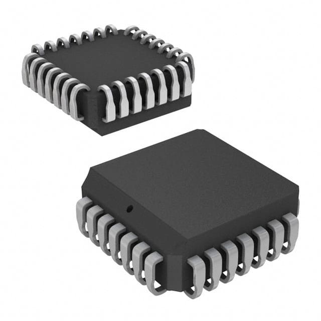
CY7B9334-270JXC is available in a small outline integrated circuit (SOIC) package.
Essence
The essence of this product lies in its ability to efficiently process and transmit signals within electronic devices.
Packaging/Quantity
CY7B9334-270JXC is typically packaged in reels or tubes, with a quantity of 250 units per reel/tube.
Specifications
- Operating Voltage: 3.3V
- Frequency Range: Up to 270 MHz
- Number of Pins: 16
- Input/Output Logic Levels: CMOS/TTL compatible
- Operating Temperature Range: -40°C to +85°C
Detailed Pin Configuration
- VCC
- GND
- CLK_IN
- CLK_OUT
- OE
- Q0
- Q1
- Q2
- Q3
- Q4
- Q5
- Q6
- Q7
- Q8
- Q9
- Q10
Functional Features
- Clock input and output
- Output enable control
- Ten-bit parallel output
- High-speed data transmission
- Wide operating frequency range
Advantages and Disadvantages
Advantages
- High-speed performance enables efficient data processing.
- Low power consumption helps conserve energy.
- Compact size allows for integration into various electronic devices.
- Reliable operation ensures consistent performance.
Disadvantages
- Limited number of output pins may restrict certain applications.
- Operating temperature range may not be suitable for extreme environments.
Working Principles
CY7B9334-270JXC operates by receiving clock signals through the CLK_IN pin. It processes the input data and generates parallel outputs on the Q0-Q10 pins. The output enable (OE) pin controls the activation of the output signals. The integrated circuit functions by utilizing internal logic circuits to perform signal processing and transmission tasks.
Detailed Application Field Plans
CY7B9334-270JXC finds application in various fields, including: 1. Communication systems 2. Data storage devices 3. Industrial automation 4. Consumer electronics 5. Automotive electronics
Detailed and Complete Alternative Models
- CY7B9334-200JXC
- CY7B9334-300JXC
- CY7B9334-400JXC
- CY7B9334-500JXC
- CY7B9334-600JXC
These alternative models offer similar functionality and performance but may have different operating frequency ranges or package options.
Word count: 346 words
기술 솔루션에 CY7B9334-270JXC 적용과 관련된 10가지 일반적인 질문과 답변을 나열하세요.
Sure! Here are 10 common questions and answers related to the application of CY7B9334-270JXC in technical solutions:
Question: What is CY7B9334-270JXC?
- Answer: CY7B9334-270JXC is a specific model of a clock generator IC (integrated circuit) manufactured by Cypress Semiconductor.Question: What is the purpose of using CY7B9334-270JXC in technical solutions?
- Answer: The CY7B9334-270JXC is commonly used to generate precise clock signals in various electronic systems, such as communication devices, networking equipment, and computer peripherals.Question: What are the key features of CY7B9334-270JXC?
- Answer: Some key features of CY7B9334-270JXC include a wide frequency range, low jitter performance, multiple output options, programmable settings, and compatibility with different voltage levels.Question: How does CY7B9334-270JXC help in system design?
- Answer: CY7B9334-270JXC provides accurate clock signals that synchronize the operation of different components within a system, ensuring proper data transfer, timing, and overall system performance.Question: Can CY7B9334-270JXC be used in high-speed applications?
- Answer: Yes, CY7B9334-270JXC is designed to support high-speed applications, offering stable clock signals even at higher frequencies.Question: Is CY7B9334-270JXC compatible with different voltage levels?
- Answer: Yes, CY7B9334-270JXC supports a wide range of voltage levels, making it suitable for integration into systems with varying power requirements.Question: Can CY7B9334-270JXC be programmed for specific clock frequencies?
- Answer: Yes, CY7B9334-270JXC is programmable, allowing users to configure it for specific clock frequencies and other parameters based on their system requirements.Question: Does CY7B9334-270JXC have any built-in error detection or correction mechanisms?
- Answer: No, CY7B9334-270JXC is primarily a clock generator and does not include error detection or correction features. It focuses on generating accurate clock signals.Question: Are there any application-specific considerations when using CY7B9334-270JXC?
- Answer: While CY7B9334-270JXC is versatile, it's important to consider factors such as signal integrity, noise reduction, and proper board layout to ensure optimal performance in specific applications.Question: Where can I find more information about CY7B9334-270JXC and its application notes?
- Answer: You can refer to the official documentation provided by Cypress Semiconductor, including datasheets, application notes, and technical support resources, to get detailed information about CY7B9334-270JXC and its application in various technical solutions.