

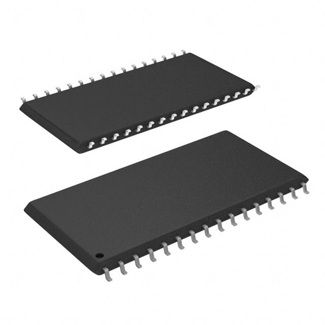
CY7C1019DV33-10ZSXIT
Product Overview
Category
The CY7C1019DV33-10ZSXIT belongs to the category of static random access memory (SRAM) chips.
Use
This product is primarily used for storing and retrieving digital information in electronic devices. It provides high-speed, non-volatile memory storage capabilities.
Characteristics
- High-speed operation: The CY7C1019DV33-10ZSXIT offers fast read and write access times, making it suitable for applications that require quick data retrieval.
- Non-volatile memory: Unlike dynamic random access memory (DRAM), SRAM retains stored data even when power is disconnected.
- Low power consumption: This chip is designed to minimize power usage, making it energy-efficient.
- Compact package: The CY7C1019DV33-10ZSXIT is available in a small form factor, allowing for space-saving integration into various electronic devices.
- Robust design: It features a durable construction that ensures reliable performance in demanding environments.
Package and Quantity
The CY7C1019DV33-10ZSXIT is typically packaged in a surface-mount technology (SMT) package, which facilitates easy installation on printed circuit boards (PCBs). The exact packaging and quantity may vary depending on the supplier or manufacturer.
Specifications
- Memory capacity: 1 Megabit (128K x 8 bits)
- Operating voltage: 3.3V
- Access time: 10 nanoseconds
- Operating temperature range: -40°C to +85°C
- Data retention: Greater than 20 years
- Interface: Parallel
Detailed Pin Configuration
The CY7C1019DV33-10ZSXIT has a total of 32 pins, each serving a specific function. Here is a detailed pin configuration:
- Chip Enable (CE)
- Output Enable (OE)
- Write Enable (WE)
- Address Inputs (A0-A16)
- Data Inputs/Outputs (DQ0-DQ7)
- Power Supply (VCC)
- Ground (GND)
Note: The remaining pins are not listed here for brevity.
Functional Features
- High-speed operation: The CY7C1019DV33-10ZSXIT offers fast read and write access times, enabling efficient data processing.
- Easy integration: It can be easily interfaced with microcontrollers or other digital devices due to its parallel interface.
- Low power consumption: This chip is designed to minimize power usage, making it suitable for battery-powered applications.
- Reliable data retention: The SRAM technology used in this product ensures data integrity even during power interruptions.
- Wide operating temperature range: The CY7C1019DV33-10ZSXIT can withstand extreme temperatures, making it suitable for various environments.
Advantages and Disadvantages
Advantages
- Fast access times enable quick data retrieval.
- Non-volatile memory ensures data retention without the need for constant power supply.
- Low power consumption prolongs battery life in portable devices.
- Compact package allows for space-saving integration.
- Robust design ensures reliable performance in challenging conditions.
Disadvantages
- Limited storage capacity compared to other memory technologies.
- Higher cost per bit compared to dynamic random access memory (DRAM).
- More susceptible to noise and interference due to its parallel interface.
Working Principles
The CY7C1019DV33-10ZSXIT utilizes static random access memory technology, which stores each bit of data in a flip-flop circuit. This allows for faster access times compared to dynamic random access memory (DRAM). When a read or write operation is initiated, the appropriate address is provided to access the desired location in the memory array. The data is then read from or written to the specified location using the parallel interface.
Detailed Application Field Plans
The CY7C1019DV33-10ZSXIT can be used in various applications that require high-speed, non-volatile memory storage. Some potential application fields include:
- Embedded Systems: This SRAM chip can be integrated into microcontrollers and embedded systems to provide fast and reliable data storage for real-time applications.
- Networking Equipment: It can be utilized in routers, switches, and other networking devices to store routing tables, buffers, and configuration data.
- Industrial Automation: The CY7C1019DV33-10ZSXIT can be employed in industrial control systems, PLCs (Programmable Logic Controllers), and robotics to store critical data and program code.
- Automotive Electronics: It can be used in automotive applications such as engine control units (ECUs), infotainment systems, and advanced driver-assistance systems (ADAS) for storing sensor data and system parameters.
Detailed and Complete Alternative Models
- CY7C1021CV33-10ZSXI
기술 솔루션에 CY7C1019DV33-10ZSXIT 적용과 관련된 10가지 일반적인 질문과 답변을 나열하세요.
Sure! Here are 10 common questions and answers related to the application of CY7C1019DV33-10ZSXIT in technical solutions:
Question: What is the maximum operating frequency of CY7C1019DV33-10ZSXIT?
Answer: The maximum operating frequency of CY7C1019DV33-10ZSXIT is 100 MHz.Question: What is the voltage supply range for this device?
Answer: The voltage supply range for CY7C1019DV33-10ZSXIT is 3.0V to 3.6V.Question: How much memory does CY7C1019DV33-10ZSXIT have?
Answer: CY7C1019DV33-10ZSXIT has a total memory capacity of 1 Megabit (128K x 8).Question: Is this device compatible with both synchronous and asynchronous operations?
Answer: Yes, CY7C1019DV33-10ZSXIT supports both synchronous and asynchronous operations.Question: What is the access time of CY7C1019DV33-10ZSXIT?
Answer: The access time of CY7C1019DV33-10ZSXIT is 10 ns.Question: Can I use this device in industrial temperature environments?
Answer: Yes, CY7C1019DV33-10ZSXIT is designed to operate in industrial temperature ranges (-40°C to +85°C).Question: Does CY7C1019DV33-10ZSXIT support multiple chip enable inputs?
Answer: No, CY7C1019DV33-10ZSXIT has a single chip enable input.Question: What is the package type of CY7C1019DV33-10ZSXIT?
Answer: CY7C1019DV33-10ZSXIT is available in a 44-pin TSOP II package.Question: Can I use this device in battery-powered applications?
Answer: Yes, CY7C1019DV33-10ZSXIT has low power consumption and can be used in battery-powered applications.Question: Does CY7C1019DV33-10ZSXIT have any built-in error correction capabilities?
Answer: No, CY7C1019DV33-10ZSXIT does not have built-in error correction capabilities.