

Encyclopedia Entry: 74AUP1G06FW5-7
Product Overview
Category
The 74AUP1G06FW5-7 belongs to the category of integrated circuits (ICs).
Use
This product is commonly used as a logic gate buffer.
Characteristics
- Low power consumption
- High-speed operation
- Wide operating voltage range
- Small package size
Package
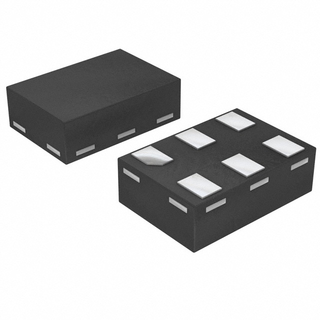
The 74AUP1G06FW5-7 is available in a small SOT353 package.
Essence
The essence of this product lies in its ability to provide buffering functionality for digital signals.
Packaging/Quantity
The 74AUP1G06FW5-7 is typically packaged in reels, with each reel containing a specific quantity of ICs. The exact quantity may vary depending on the manufacturer.
Specifications
- Supply Voltage Range: 0.8V to 3.6V
- Input Voltage Range: -0.5V to VCC + 0.5V
- Output Voltage Range: -0.5V to VCC + 0.5V
- Operating Temperature Range: -40°C to +85°C
Detailed Pin Configuration
The 74AUP1G06FW5-7 has the following pin configuration:
____
   IN |    | OUT
      |    |
   GND|____| VCC
Functional Features
- Buffering: The 74AUP1G06FW5-7 acts as a buffer, amplifying and stabilizing digital signals.
- Signal Inversion: It can also invert the input signal, providing both non-inverted and inverted outputs.
Advantages
- Low Power Consumption: The product's low power consumption makes it suitable for battery-powered devices.
- High-Speed Operation: Its high-speed operation allows for efficient signal processing.
- Wide Operating Voltage Range: The wide operating voltage range enhances compatibility with various systems.
- Small Package Size: The compact package size enables space-saving designs.
Disadvantages
- Limited Output Current: The product has a limited output current capability, which may restrict its use in certain applications.
- Single Input: It only supports a single input, limiting its versatility in complex circuit designs.
Working Principles
The 74AUP1G06FW5-7 operates based on the principles of CMOS (Complementary Metal-Oxide-Semiconductor) technology. It utilizes MOSFET transistors to amplify and control the digital signals passing through it.
Detailed Application Field Plans
The 74AUP1G06FW5-7 finds application in various fields, including: 1. Consumer Electronics: Used in smartphones, tablets, and portable media players for signal buffering and level shifting. 2. Automotive: Employed in automotive electronics for signal conditioning and interfacing. 3. Industrial Automation: Utilized in industrial control systems for signal amplification and inversion. 4. Communication Systems: Integrated into communication devices for signal processing and line driving.
Detailed and Complete Alternative Models
- 74AUP1G06GW5-7: Similar to the 74AUP1G06FW5-7, but with a different package type.
- 74LVC1G06GW5-7: Offers similar functionality with improved noise immunity and higher output current capability.
- SN74LVC1G06DBVR: An alternative model from a different manufacturer, providing comparable features.
In conclusion, the 74AUP1G06FW5-7 is a versatile logic gate buffer IC that offers low power consumption, high-speed operation, and a wide operating voltage range. While it has limitations in terms of output current and input options, it finds applications in various fields such as consumer electronics, automotive, industrial automation, and communication systems. Alternative models like the 74AUP1G06GW5-7, 74LVC1G06GW5-7, and SN74LVC1G06DBVR provide similar functionality with slight variations.
기술 솔루션에 74AUP1G06FW5-7 적용과 관련된 10가지 일반적인 질문과 답변을 나열하세요.
Sure! Here are 10 common questions and answers related to the application of the 74AUP1G06FW5-7 in technical solutions:
Q1: What is the 74AUP1G06FW5-7? A1: The 74AUP1G06FW5-7 is a single unbuffered inverter gate with open-drain output, commonly used in digital logic circuits.
Q2: What is the operating voltage range of the 74AUP1G06FW5-7? A2: The 74AUP1G06FW5-7 operates within a voltage range of 0.8V to 3.6V.
Q3: What is the maximum output current of the 74AUP1G06FW5-7? A3: The maximum output current of the 74AUP1G06FW5-7 is typically 32mA.
Q4: Can the 74AUP1G06FW5-7 be used as a level shifter? A4: Yes, the 74AUP1G06FW5-7 can be used as a level shifter to convert signals between different voltage levels.
Q5: What is the propagation delay of the 74AUP1G06FW5-7? A5: The propagation delay of the 74AUP1G06FW5-7 is typically around 2.5ns.
Q6: Is the 74AUP1G06FW5-7 suitable for high-speed applications? A6: Yes, the 74AUP1G06FW5-7 is designed for high-speed operation and can be used in various high-frequency applications.
Q7: Can the 74AUP1G06FW5-7 be used in battery-powered devices? A7: Yes, the 74AUP1G06FW5-7 has a low power consumption and can be used in battery-powered devices.
Q8: What is the package type of the 74AUP1G06FW5-7? A8: The 74AUP1G06FW5-7 is available in a small SOT353 package.
Q9: Can the 74AUP1G06FW5-7 be used in both digital and analog circuits? A9: No, the 74AUP1G06FW5-7 is specifically designed for digital logic applications and may not be suitable for analog circuits.
Q10: Are there any recommended application circuits for the 74AUP1G06FW5-7? A10: Yes, the datasheet of the 74AUP1G06FW5-7 provides several recommended application circuits that can be used as a reference for different use cases.
Please note that these answers are general and may vary depending on specific design requirements and conditions. It's always recommended to refer to the datasheet and consult with technical experts for accurate information.