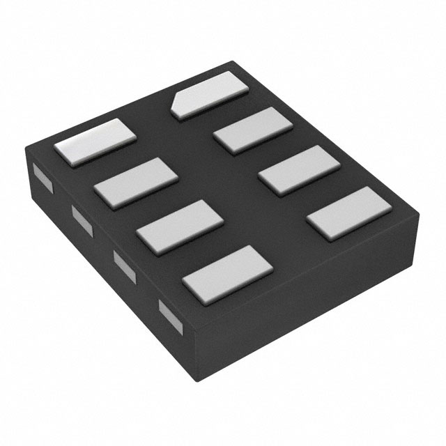
74LVC2G00HK3-7
Basic Information Overview
- Category: Integrated Circuit (IC)
- Use: Logic Gate
- Characteristics: Dual 2-Input NAND Gate
- Package: SOT353 (SC-88A)
- Essence: High-Speed CMOS Technology
- Packaging/Quantity: Tape and Reel, 3000 pieces per reel
Specifications
- Supply Voltage Range: 1.65V to 5.5V
- Input Voltage Range: -0.5V to VCC + 0.5V
- Output Voltage Range: 0V to VCC
- Operating Temperature Range: -40°C to +125°C
- Propagation Delay: 4.3ns (typical) at 3.3V supply voltage
Detailed Pin Configuration
The 74LVC2G00HK3-7 has a total of 5 pins: 1. Pin 1: Input A 2. Pin 2: Input B 3. Pin 3: Ground (GND) 4. Pin 4: Output Y 5. Pin 5: Power Supply (VCC)
Functional Features
- Dual 2-Input NAND Gate: The IC consists of two independent NAND gates, each with two inputs and one output.
- High-Speed Operation: Utilizing high-speed CMOS technology, the IC offers fast propagation delay, making it suitable for applications requiring quick response times.
- Wide Voltage Range: The IC can operate within a wide supply voltage range, allowing flexibility in various electronic systems.
- Low Power Consumption: The device is designed to consume low power, making it energy-efficient.
Advantages and Disadvantages
Advantages: - Compact Size: The SOT353 package enables a small footprint, ideal for space-constrained designs. - Versatile: The dual NAND gate configuration provides flexibility in designing logic circuits. - High-Speed Performance: The IC offers fast propagation delay, enhancing overall system performance.
Disadvantages: - Limited Input/Output Configuration: The IC only supports two inputs and one output per gate, which may restrict certain complex circuit designs. - Sensitivity to Voltage Fluctuations: The device may be susceptible to malfunctions or errors if the supply voltage is not stable.
Working Principles
The 74LVC2G00HK3-7 operates based on the principles of digital logic. Each NAND gate within the IC performs a logical AND operation on its two input signals and then negates the result, providing the output signal. The high-speed CMOS technology employed ensures efficient switching between logic states.
Detailed Application Field Plans
The 74LVC2G00HK3-7 finds applications in various electronic systems, including but not limited to: 1. Microcontrollers and Microprocessors 2. Communication Systems 3. Industrial Control Systems 4. Automotive Electronics 5. Consumer Electronics
Detailed and Complete Alternative Models
Some alternative models that can be considered as replacements for the 74LVC2G00HK3-7 include: 1. SN74LVC2G00DBVR by Texas Instruments 2. MC74VHC1G00DTT1G by ON Semiconductor 3. 74AHC2G00GW by NXP Semiconductors 4. CD74HC00M by Texas Instruments 5. TC7SZ00FU by Toshiba Semiconductor
Please note that the suitability of these alternatives depends on specific application requirements and compatibility with the existing circuit design.
Word count: 422 words
기술 솔루션에 74LVC2G00HK3-7 적용과 관련된 10가지 일반적인 질문과 답변을 나열하세요.
Sure! Here are 10 common questions and answers related to the application of 74LVC2G00HK3-7 in technical solutions:
Q: What is the 74LVC2G00HK3-7? A: The 74LVC2G00HK3-7 is a dual 2-input NAND gate integrated circuit (IC) that operates at a voltage range of 1.65V to 5.5V.
Q: What are the typical applications of the 74LVC2G00HK3-7? A: The 74LVC2G00HK3-7 can be used in various digital logic applications, such as signal amplification, level shifting, and general-purpose logic functions.
Q: What is the maximum operating frequency of the 74LVC2G00HK3-7? A: The maximum operating frequency of the 74LVC2G00HK3-7 is typically around 200 MHz.
Q: What is the power supply voltage range for the 74LVC2G00HK3-7? A: The 74LVC2G00HK3-7 can operate within a power supply voltage range of 1.65V to 5.5V.
Q: Can the 74LVC2G00HK3-7 handle both CMOS and TTL input levels? A: Yes, the 74LVC2G00HK3-7 is compatible with both CMOS and TTL input levels.
Q: Does the 74LVC2G00HK3-7 have built-in protection against electrostatic discharge (ESD)? A: Yes, the 74LVC2G00HK3-7 has built-in ESD protection, which helps safeguard the IC against damage during handling and operation.
Q: What is the output drive capability of the 74LVC2G00HK3-7? A: The 74LVC2G00HK3-7 has a typical output drive capability of ±24 mA.
Q: Can the 74LVC2G00HK3-7 be used in battery-powered applications? A: Yes, the 74LVC2G00HK3-7 can operate at low power supply voltages, making it suitable for battery-powered applications.
Q: Is the 74LVC2G00HK3-7 available in different package options? A: Yes, the 74LVC2G00HK3-7 is available in various package options, such as SOT353 and XSON6.
Q: Where can I find more detailed information about the 74LVC2G00HK3-7? A: You can refer to the datasheet provided by the manufacturer or visit their official website for more detailed information about the 74LVC2G00HK3-7.


