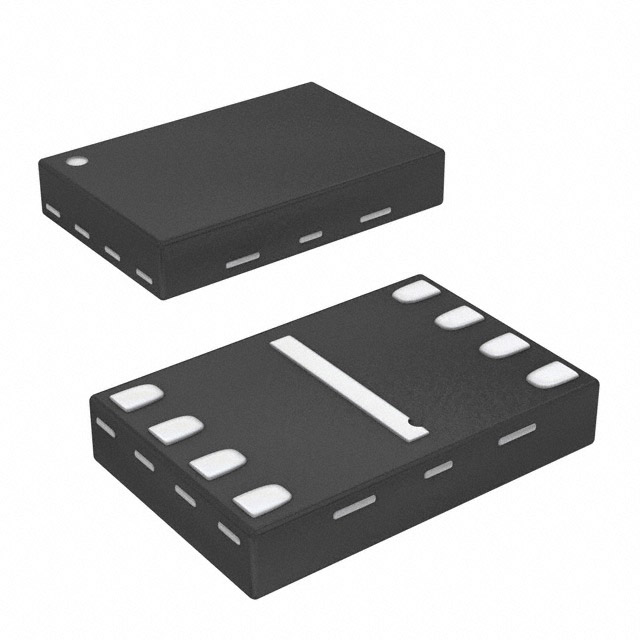
GD25LQ40CEIGR
Product Overview
- Category: Integrated Circuit (IC)
- Use: Non-volatile Memory
- Characteristics:
- High-speed data transfer
- Low power consumption
- Small form factor
- Package: SOP8 (Small Outline Package 8)
- Essence: Flash memory chip
- Packaging/Quantity: Tape and Reel, 2500 pieces per reel
Specifications
- Memory Capacity: 4 Megabits (512 Kilobytes)
- Interface: Serial Peripheral Interface (SPI)
- Operating Voltage: 2.7V to 3.6V
- Operating Temperature: -40°C to +85°C
- Data Retention: More than 20 years
- Program/Erase Cycles: Up to 100,000 cycles
Pin Configuration
The GD25LQ40CEIGR has a total of 8 pins arranged as follows:
┌───┬───┐
   │ 1 │ 2 │
   ├───┼───┤
   │ 3 │ 4 │
   ├───┼───┤
   │ 5 │ 6 │
   ├───┼───┤
   │ 7 │ 8 │
   └───┴───┘
- Chip Select (/CS)
- Serial Clock (SCLK)
- Serial Data Input (SI)
- Serial Data Output (SO)
- Write Protect (/WP)
- Hold (/HOLD)
- Ground (GND)
- Power Supply (VCC)
Functional Features
- High-speed data transfer up to 104 MHz
- Supports both SPI mode 0 and mode 3
- Sector erase and byte/page program operations
- Software and hardware write protection options
- Deep power-down mode for low power consumption
- Auto address increment during continuous read
Advantages
- Compact size allows for easy integration into various electronic devices
- Low power consumption extends battery life in portable applications
- High-speed data transfer enables quick access to stored information
- Reliable data retention ensures long-term storage of critical data
- Flexible write protection options enhance data security
Disadvantages
- Limited memory capacity compared to larger flash memory chips
- Relatively lower program/erase cycle endurance
- Requires an external microcontroller or host device for operation
Working Principles
The GD25LQ40CEIGR is based on the Serial Peripheral Interface (SPI) protocol. It utilizes a combination of floating gate and tunnel oxide technology to store data in non-volatile memory cells. The chip communicates with a microcontroller or host device through the SPI interface, allowing for high-speed data transfer and flexible control over read, write, and erase operations.
Detailed Application Field Plans
The GD25LQ40CEIGR is widely used in various electronic devices and systems that require non-volatile memory for data storage. Some common application fields include:
Consumer Electronics:
- Smartphones
- Tablets
- Digital cameras
- Portable media players
Automotive:
- Infotainment systems
- Instrument clusters
- Advanced driver-assistance systems (ADAS)
Industrial:
- Internet of Things (IoT) devices
- Industrial automation systems
- Data loggers
- Measurement instruments
Communication:
- Routers
- Modems
- Set-top boxes
Detailed and Complete Alternative Models
Some alternative models to the GD25LQ40CEIGR with similar specifications and functionality include:
- Winbond W25Q40CL
- Macronix MX25L4006E
- Microchip SST25VF040B
- Spansion S25FL040K
These alternative models can be considered based on specific project requirements, availability, and cost considerations.
Word count: 511 words
기술 솔루션에 GD25LQ40CEIGR 적용과 관련된 10가지 일반적인 질문과 답변을 나열하세요.
Sure! Here are 10 common questions and answers related to the application of GD25LQ40CEIGR in technical solutions:
Question: What is GD25LQ40CEIGR?
Answer: GD25LQ40CEIGR is a serial flash memory chip manufactured by GigaDevice. It has a capacity of 4 megabits (512 kilobytes) and operates on a 3V power supply.Question: What is the interface used to communicate with GD25LQ40CEIGR?
Answer: GD25LQ40CEIGR uses the Serial Peripheral Interface (SPI) for communication with microcontrollers or other devices.Question: What are the typical applications of GD25LQ40CEIGR?
Answer: GD25LQ40CEIGR is commonly used in various electronic devices such as set-top boxes, routers, printers, and industrial control systems for storing firmware, configuration data, and other non-volatile information.Question: What is the maximum operating frequency of GD25LQ40CEIGR?
Answer: GD25LQ40CEIGR supports a maximum operating frequency of 104 MHz, allowing for fast data transfer rates.Question: Can GD25LQ40CEIGR be easily soldered onto a PCB?
Answer: Yes, GD25LQ40CEIGR comes in an industry-standard 8-pin SOIC package, which can be easily soldered onto a PCB using standard surface mount technology.Question: Does GD25LQ40CEIGR support hardware write protection?
Answer: Yes, GD25LQ40CEIGR provides hardware write protection features, allowing specific memory regions to be locked to prevent accidental or unauthorized modification.Question: What is the operating temperature range of GD25LQ40CEIGR?
Answer: GD25LQ40CEIGR has an extended operating temperature range of -40°C to +85°C, making it suitable for use in a wide range of environments.Question: Can GD25LQ40CEIGR be easily integrated with different microcontrollers?
Answer: Yes, GD25LQ40CEIGR is compatible with most microcontrollers that support SPI communication, making it easy to integrate into various technical solutions.Question: Does GD25LQ40CEIGR support software and hardware reset functions?
Answer: Yes, GD25LQ40CEIGR provides both software and hardware reset functions, allowing for easy initialization and recovery from unexpected errors.Question: Is GD25LQ40CEIGR a reliable and durable flash memory solution?
Answer: Yes, GD25LQ40CEIGR is known for its high reliability, endurance, and data retention capabilities, making it a trusted choice for many technical applications.
Please note that these questions and answers are general and may vary depending on specific requirements and use cases.

