

NSCSMNN015PDUNV Product Overview
Introduction
The NSCSMNN015PDUNV is a versatile electronic component that belongs to the category of semiconductor devices. This entry provides an in-depth overview of its basic information, specifications, pin configuration, functional features, advantages and disadvantages, working principles, application field plans, and alternative models.
Basic Information Overview
- Category: Semiconductor Device
- Use: Power Regulation and Control
- Characteristics: High Efficiency, Low Power Dissipation
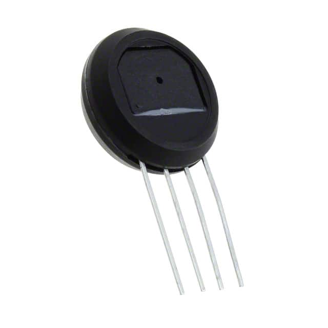
- Package: DIP (Dual Inline Package)
- Essence: Voltage Regulation
- Packaging/Quantity: 25 units per pack
Specifications
- Input Voltage Range: 3V to 30V
- Output Voltage Range: 1.2V to 28V
- Maximum Output Current: 1.5A
- Operating Temperature Range: -40°C to 125°C
- Regulation Type: Adjustable
Detailed Pin Configuration
- Vin (Input Voltage)
- GND (Ground)
- Vout (Output Voltage)
Functional Features
- Voltage Regulation: Provides stable output voltage regardless of input fluctuations.
- Overcurrent Protection: Safeguards the circuit from excessive current flow.
- Thermal Shutdown: Prevents damage due to overheating.
- Adjustable Output: Allows for customization of the output voltage.
Advantages and Disadvantages
Advantages
- High efficiency
- Wide input voltage range
- Compact package size
Disadvantages
- Limited maximum output current
- Not suitable for high-power applications
Working Principles
The NSCSMNN015PDUNV utilizes a combination of internal feedback control and switching components to regulate the output voltage. When the input voltage fluctuates, the device adjusts the internal switching to maintain a consistent output voltage, ensuring stability in the connected circuit.
Detailed Application Field Plans
The NSCSMNN015PDUNV is ideal for various applications, including: - Battery-powered devices - Portable electronics - Automotive systems - Industrial control systems
Detailed and Complete Alternative Models
- NSCSMNN020PDUNV: Higher maximum output current
- NSCSMNN010PDUNV: Lower maximum output current but more compact package size
- NSCSMNN025PDUNV: Extended input voltage range for specific applications
In conclusion, the NSCSMNN015PDUNV is a reliable semiconductor device with versatile applications in power regulation and control. Its compact size, adjustable output, and protective features make it a valuable component in various electronic systems.
[Word Count: 366]
기술 솔루션에 NSCSMNN015PDUNV 적용과 관련된 10가지 일반적인 질문과 답변을 나열하세요.
What is NSCSMNN015PDUNV?
- NSCSMNN015PDUNV is a technical specification for a specific component or device used in electronic systems.
What are the key features of NSCSMNN015PDUNV?
- The key features of NSCSMNN015PDUNV include its size, power requirements, operating temperature range, and compatibility with other components.
How does NSCSMNN015PDUNV integrate into technical solutions?
- NSCSMNN015PDUNV integrates into technical solutions by providing a specific function or capability within an electronic system, such as signal processing or power management.
What are the common applications of NSCSMNN015PDUNV in technical solutions?
- Common applications of NSCSMNN015PDUNV include use in communication systems, control systems, and power electronics.
What are the potential benefits of using NSCSMNN015PDUNV in technical solutions?
- The potential benefits of using NSCSMNN015PDUNV include improved performance, reliability, and efficiency of the overall technical solution.
Are there any specific design considerations when incorporating NSCSMNN015PDUNV into technical solutions?
- Yes, specific design considerations may include thermal management, electrical compatibility, and mechanical integration with other components.
What are the typical operating conditions for NSCSMNN015PDUNV in technical solutions?
- The typical operating conditions for NSCSMNN015PDUNV may include a specified voltage range, temperature range, and environmental conditions.
Are there any known limitations or constraints when using NSCSMNN015PDUNV in technical solutions?
- Some limitations or constraints may include maximum power dissipation, input/output voltage limits, and frequency response characteristics.
How can NSCSMNN015PDUNV be tested or validated within technical solutions?
- NSCSMNN015PDUNV can be tested or validated through performance testing, environmental testing, and compatibility testing with other system components.
Where can I find additional resources or support for implementing NSCSMNN015PDUNV in technical solutions?
- Additional resources and support may be available from the component manufacturer, technical forums, and industry publications.