

ADC1413S080HN/C1,5
Product Overview
Category
The ADC1413S080HN/C1,5 belongs to the category of Analog-to-Digital Converters (ADCs).
Use
This product is primarily used for converting analog signals into digital data.
Characteristics
- High precision and accuracy
- Fast conversion speed
- Low power consumption
- Wide input voltage range
Package
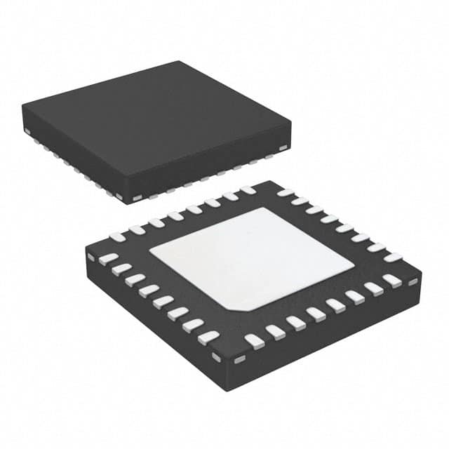
The ADC1413S080HN/C1,5 is available in a compact package, suitable for surface mount technology (SMT) applications.
Essence
The essence of this product lies in its ability to accurately convert analog signals into digital format, enabling further processing and analysis.
Packaging/Quantity
The ADC1413S080HN/C1,5 is typically packaged in reels or trays, with a quantity of 250 units per reel/tray.
Specifications
- Resolution: 14 bits
- Sampling Rate: 1 MSPS (Mega Samples Per Second)
- Input Voltage Range: ±10V
- Power Supply: 3.3V
- Operating Temperature Range: -40°C to +85°C
Detailed Pin Configuration
The ADC1413S080HN/C1,5 has the following pin configuration:
- VDD: Power supply voltage
- VREF: Reference voltage input
- AGND: Analog ground
- VIN: Analog input voltage
- CLK: Clock input
- CS: Chip select input
- DOUT: Digital output
- DGND: Digital ground
Functional Features
- High-resolution conversion
- Low noise and distortion
- Built-in voltage reference
- Serial interface for easy integration
- Programmable gain amplifier (PGA)
Advantages and Disadvantages
Advantages
- High precision and accuracy
- Fast conversion speed
- Low power consumption
- Wide input voltage range
- Compact package for space-constrained applications
Disadvantages
- Limited sampling rate compared to some higher-end ADCs
- Requires external voltage reference for optimal performance
Working Principles
The ADC1413S080HN/C1,5 utilizes a successive approximation register (SAR) architecture to convert analog signals into digital data. It samples the input voltage at a high rate and performs a series of comparisons to determine the digital representation of the analog signal.
Detailed Application Field Plans
The ADC1413S080HN/C1,5 finds applications in various fields, including:
- Industrial automation: Precise measurement and control systems
- Medical devices: Vital sign monitoring, diagnostic equipment
- Communications: Signal processing, baseband applications
- Test and measurement: Data acquisition, instrumentation
Detailed and Complete Alternative Models
- ADC1423S100HN/C2,5: Higher resolution (14 bits), faster sampling rate (2 MSPS)
- ADC1210S060HN/C1,5: Lower resolution (12 bits), lower power consumption
- ADC1616S120HN/C3,5: Higher resolution (16 bits), wider input voltage range
These alternative models offer different specifications and features to cater to specific application requirements.
In conclusion, the ADC1413S080HN/C1,5 is a high-precision analog-to-digital converter with fast conversion speed and low power consumption. Its compact package and wide input voltage range make it suitable for various applications in industrial automation, medical devices, communications, and test and measurement. While it has some limitations in terms of sampling rate and external voltage reference requirement, there are alternative models available with different specifications to meet specific needs.
기술 솔루션에 ADC1413S080HN/C1,5 적용과 관련된 10가지 일반적인 질문과 답변을 나열하세요.
Question: What is the ADC1413S080HN/C1,5 used for?
Answer: The ADC1413S080HN/C1,5 is an analog-to-digital converter (ADC) commonly used in technical solutions to convert analog signals into digital data.Question: What is the resolution of the ADC1413S080HN/C1,5?
Answer: The ADC1413S080HN/C1,5 has a resolution of 14 bits, allowing for high-precision conversion of analog signals.Question: What is the sampling rate of the ADC1413S080HN/C1,5?
Answer: The ADC1413S080HN/C1,5 has a maximum sampling rate of 80 kilosamples per second (ksps), enabling fast and accurate signal conversion.Question: What is the input voltage range of the ADC1413S080HN/C1,5?
Answer: The ADC1413S080HN/C1,5 has a single-ended input voltage range of 0 to Vref, where Vref is the reference voltage provided to the ADC.Question: Does the ADC1413S080HN/C1,5 support differential inputs?
Answer: No, the ADC1413S080HN/C1,5 only supports single-ended inputs.Question: What is the power supply voltage range for the ADC1413S080HN/C1,5?
Answer: The ADC1413S080HN/C1,5 operates with a power supply voltage range of 2.7V to 5.5V, making it compatible with various power sources.Question: Can the ADC1413S080HN/C1,5 be used in low-power applications?
Answer: Yes, the ADC1413S080HN/C1,5 features a low-power mode that reduces power consumption during idle periods, making it suitable for low-power applications.Question: Does the ADC1413S080HN/C1,5 have built-in reference voltage options?
Answer: No, the ADC1413S080HN/C1,5 requires an external reference voltage to be provided for accurate signal conversion.Question: What is the interface used to communicate with the ADC1413S080HN/C1,5?
Answer: The ADC1413S080HN/C1,5 utilizes a serial peripheral interface (SPI) for communication with microcontrollers or other digital devices.Question: Are there any evaluation boards or development kits available for the ADC1413S080HN/C1,5?
Answer: Yes, the manufacturer provides evaluation boards and development kits that can be used to test and integrate the ADC1413S080HN/C1,5 into technical solutions.