

SPB100N08S2L-07
Introduction
The SPB100N08S2L-07 is a power MOSFET belonging to the category of electronic components. It is widely used in various applications due to its unique characteristics and functional features.
Basic Information Overview
- Category: Electronic Component
- Use: Power MOSFET for electronic circuits
- Characteristics: High power handling capacity, low on-resistance, efficient switching capabilities
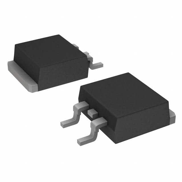
- Package: TO-263-3 (D2PAK) package
- Essence: Efficient power management and control
- Packaging/Quantity: Typically packaged in reels or tubes, quantity varies based on supplier
Specifications
- Voltage Rating: 80V
- Current Rating: 100A
- On-Resistance: 8mΩ
- Gate Charge: 40nC
- Operating Temperature Range: -55°C to 175°C
Detailed Pin Configuration
The SPB100N08S2L-07 follows the standard pin configuration for a TO-263-3 package: 1. Source (S) 2. Gate (G) 3. Drain (D)
Functional Features
- High Power Handling: Capable of managing high currents and voltages effectively.
- Low On-Resistance: Minimizes power loss and heat generation during operation.
- Efficient Switching: Enables rapid switching transitions, suitable for various power control applications.
Advantages and Disadvantages
Advantages: - High power handling capacity - Low on-resistance - Efficient power management
Disadvantages: - Sensitive to static electricity - Requires careful handling during installation
Working Principles
The SPB100N08S2L-07 operates based on the principles of field-effect transistors, utilizing the control of electric fields to modulate the conductivity of the semiconductor material.
Detailed Application Field Plans
The SPB100N08S2L-07 finds extensive use in the following application fields: - Switching power supplies - Motor control systems - Inverters and converters - Automotive electronics - Industrial automation
Detailed and Complete Alternative Models
- Alternative Model 1: SPB120N08S2L-07
- Voltage Rating: 120V
- Current Rating: 100A
- On-Resistance: 6mΩ
- Alternative Model 2: SPB080N08S2L-07
- Voltage Rating: 80V
- Current Rating: 80A
- On-Resistance: 10mΩ
In conclusion, the SPB100N08S2L-07 power MOSFET offers high-performance characteristics and versatile applications, making it an essential component in modern electronic systems.
Word Count: 366
기술 솔루션에 SPB100N08S2L-07 적용과 관련된 10가지 일반적인 질문과 답변을 나열하세요.
What is the maximum drain-source voltage rating of SPB100N08S2L-07?
- The maximum drain-source voltage rating of SPB100N08S2L-07 is 80V.
What is the continuous drain current rating of SPB100N08S2L-07?
- The continuous drain current rating of SPB100N08S2L-07 is 100A.
What is the on-resistance of SPB100N08S2L-07?
- The on-resistance of SPB100N08S2L-07 is typically 8mΩ at Vgs = 10V.
Can SPB100N08S2L-07 be used in automotive applications?
- Yes, SPB100N08S2L-07 is suitable for automotive applications.
What is the operating temperature range of SPB100N08S2L-07?
- The operating temperature range of SPB100N08S2L-07 is -55°C to 175°C.
Is SPB100N08S2L-07 suitable for high-power switching applications?
- Yes, SPB100N08S2L-07 is well-suited for high-power switching applications.
Does SPB100N08S2L-07 require a heat sink for thermal management?
- Depending on the application and power dissipation, a heat sink may be required for optimal thermal management.
What type of package does SPB100N08S2L-07 come in?
- SPB100N08S2L-07 is available in a TO-263-2 (D2PAK) package.
Can SPB100N08S2L-07 be used in parallel to increase current handling capability?
- Yes, SPB100N08S2L-07 can be used in parallel to increase current handling capability.
Are there any recommended application circuits or reference designs for using SPB100N08S2L-07?
- Yes, there are recommended application circuits and reference designs available in the datasheet for utilizing SPB100N08S2L-07 in various technical solutions.