

SPB80N06S2L-07
Introduction
The SPB80N06S2L-07 is a power MOSFET belonging to the category of electronic components. This device is commonly used in various applications due to its unique characteristics and functional features. In this entry, we will provide an overview of the basic information, specifications, pin configuration, functional features, advantages and disadvantages, working principles, application field plans, and alternative models of the SPB80N06S2L-07.
Basic Information Overview
- Category: Electronic Components
- Use: Power MOSFET for switching applications
- Characteristics: High voltage capability, low on-resistance, fast switching speed
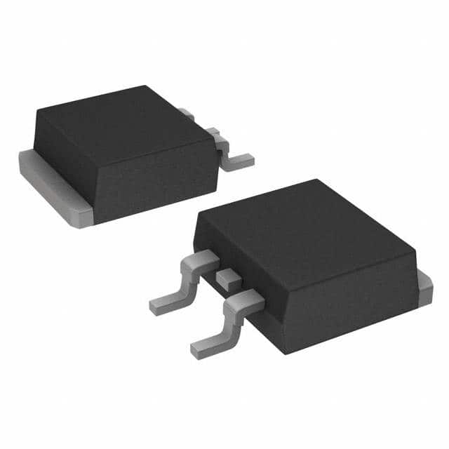
- Package: TO-263-2 (D2PAK)
- Essence: Efficient power management
- Packaging/Quantity: Typically packaged in reels or tubes, quantity varies based on manufacturer
Specifications
- Voltage Rating: 60V
- Continuous Drain Current: 80A
- On-Resistance: 8.5mΩ
- Gate Threshold Voltage: 2V
- Power Dissipation: 200W
Detailed Pin Configuration
The SPB80N06S2L-07 typically follows the standard pin configuration for a D2PAK package: 1. Gate (G) 2. Drain (D) 3. Source (S)
Functional Features
- High voltage capability allows for use in various power applications
- Low on-resistance minimizes power loss and heat generation
- Fast switching speed enables efficient power management
Advantages and Disadvantages
Advantages
- High voltage capability suitable for diverse applications
- Low on-resistance leads to improved efficiency
- Fast switching speed enhances power management
Disadvantages
- Higher cost compared to lower-rated MOSFETs
- May require additional circuitry for optimal performance in some applications
Working Principles
The SPB80N06S2L-07 operates based on the principle of field-effect transistors, where the voltage applied to the gate terminal controls the flow of current between the drain and source terminals. By modulating the gate voltage, the MOSFET can efficiently switch high currents with minimal power loss.
Detailed Application Field Plans
The SPB80N06S2L-07 finds extensive use in the following application fields: - Switching power supplies - Motor control - LED lighting - Automotive electronics - Industrial automation
Detailed and Complete Alternative Models
Some alternative models to the SPB80N06S2L-07 include: - IRF840 - FDP8878 - STP80NF03L
In conclusion, the SPB80N06S2L-07 power MOSFET offers high voltage capability, low on-resistance, and fast switching speed, making it suitable for a wide range of power management applications across various industries.
[Word Count: 398]
기술 솔루션에 SPB80N06S2L-07 적용과 관련된 10가지 일반적인 질문과 답변을 나열하세요.
What is the SPB80N06S2L-07?
- The SPB80N06S2L-07 is a power MOSFET transistor designed for high current applications.
What is the maximum voltage and current rating of SPB80N06S2L-07?
- The maximum voltage rating is 60V, and the continuous drain current rating is 80A.
What are the typical applications of SPB80N06S2L-07?
- It is commonly used in power supplies, motor control, and other high-current switching applications.
What are the key features of SPB80N06S2L-07?
- Some key features include low on-resistance, fast switching speed, and high ruggedness.
What is the thermal resistance of SPB80N06S2L-07?
- The typical junction-to-case thermal resistance is 0.75°C/W.
Is SPB80N06S2L-07 suitable for automotive applications?
- Yes, it is suitable for automotive applications due to its high current handling capability and rugged design.
Can SPB80N06S2L-07 be used in parallel to handle higher currents?
- Yes, multiple SPB80N06S2L-07 transistors can be used in parallel to increase the current-handling capacity.
Does SPB80N06S2L-07 require a heat sink for operation?
- Depending on the application and current levels, a heat sink may be required to ensure proper thermal management.
What are the recommended gate drive voltage and current for SPB80N06S2L-07?
- The recommended gate drive voltage is typically 10V, and the gate drive current should be sufficient to charge and discharge the gate capacitance quickly.
Are there any specific layout considerations when using SPB80N06S2L-07 in a circuit?
- Proper PCB layout and attention to high-current traces and thermal management are important for optimal performance and reliability.