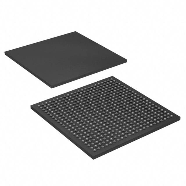
10CL040YF484I7G
Product Overview
- Category: Integrated Circuit (IC)
- Use: This IC is used for various electronic applications, including signal processing, control systems, and communication devices.
- Characteristics: The 10CL040YF484I7G IC offers high performance, low power consumption, and excellent reliability. It is designed to meet the demands of modern electronic systems.
- Package: The IC comes in a compact and durable package, ensuring easy handling and protection against external factors such as moisture and temperature variations.
- Essence: The essence of the 10CL040YF484I7G IC lies in its ability to provide efficient and reliable electronic functionality within a small form factor.
- Packaging/Quantity: The IC is typically packaged individually and is available in various quantities depending on the manufacturer's specifications.
Specifications
- Model Number: 10CL040YF484I7G
- Package Type: 484-ball FineLine BGA
- Operating Voltage: 3.3V
- Operating Temperature Range: -40°C to +85°C
- Number of Pins: 484
- Clock Frequency: Up to 500 MHz
- Logic Elements: 40,000
- Embedded Memory: 1,800 Kbits
- I/O Standards: LVCMOS, LVTTL, SSTL, HSTL, LVDS, RSDS
Detailed Pin Configuration
The 10CL040YF484I7G IC has a total of 484 pins arranged in a specific configuration. Please refer to the datasheet provided by the manufacturer for the detailed pinout diagram and description.
Functional Features
- High-speed signal processing capabilities
- Flexible I/O standards support
- Low power consumption
- Built-in memory for data storage
- Configurable logic elements for customization
- Support for various communication protocols
- On-chip clock management
Advantages and Disadvantages
Advantages
- High performance and reliability
- Compact size for space-constrained applications
- Wide operating temperature range
- Versatile I/O standards support
- Configurable logic elements offer flexibility in design
Disadvantages
- Limited embedded memory capacity
- Higher cost compared to simpler ICs
- Requires expertise in programming and configuration
Working Principles
The 10CL040YF484I7G IC operates based on the principles of digital logic. It consists of configurable logic elements, memory blocks, and I/O interfaces. The logic elements can be programmed to perform specific functions, allowing the IC to adapt to different application requirements. The embedded memory provides storage for data processing, while the I/O interfaces enable communication with external devices.
Detailed Application Field Plans
The 10CL040YF484I7G IC finds applications in various fields, including:
- Industrial automation systems
- Communication equipment
- Automotive electronics
- Medical devices
- Consumer electronics
- Aerospace and defense systems
In these fields, the IC is utilized for tasks such as signal processing, control systems, data communication, and sensor interfacing.
Detailed and Complete Alternative Models
Model: 10CL025YF484I7G
- Package Type: 484-ball FineLine BGA
- Logic Elements: 25,000
- Embedded Memory: 900 Kbits
Model: 10CL080YF484I7G
- Package Type: 484-ball FineLine BGA
- Logic Elements: 80,000
- Embedded Memory: 3,600 Kbits
Model: 10CL120YF484I7G
- Package Type: 484-ball FineLine BGA
- Logic Elements: 120,000
- Embedded Memory: 5,400 Kbits
These alternative models offer different logic element counts and memory capacities, allowing users to choose the most suitable option for their specific application requirements.
Note: The above information is provided as an example and may vary depending on the manufacturer and product availability.
Word Count: 550
기술 솔루션에 10CL040YF484I7G 적용과 관련된 10가지 일반적인 질문과 답변을 나열하세요.
Sure! Here are 10 common questions and answers related to the application of 10CL040YF484I7G in technical solutions:
Q: What is 10CL040YF484I7G? A: 10CL040YF484I7G is a specific model number for an FPGA (Field-Programmable Gate Array) manufactured by Intel.
Q: What is an FPGA used for? A: FPGAs are programmable integrated circuits that can be configured to perform various tasks, such as digital signal processing, data encryption, or hardware acceleration.
Q: What are the key features of 10CL040YF484I7G? A: Some key features of 10CL040YF484I7G include 40,000 logic elements, 2,618 Kbits of embedded memory, and support for various I/O standards.
Q: Can 10CL040YF484I7G be used in industrial applications? A: Yes, 10CL040YF484I7G is suitable for industrial applications due to its robustness, reliability, and support for extended temperature ranges.
Q: Is 10CL040YF484I7G compatible with popular development tools? A: Yes, 10CL040YF484I7G is compatible with widely-used development tools like Intel Quartus Prime, which simplifies the design and programming process.
Q: Can 10CL040YF484I7G be reprogrammed after deployment? A: Yes, FPGAs like 10CL040YF484I7G can be reprogrammed multiple times, allowing for flexibility and adaptability in the field.
Q: What interfaces does 10CL040YF484I7G support? A: 10CL040YF484I7G supports various interfaces, including PCIe, Ethernet, USB, SPI, I2C, and UART, making it versatile for different connectivity requirements.
Q: Can 10CL040YF484I7G be used in high-performance computing applications? A: Yes, 10CL040YF484I7G is suitable for high-performance computing applications due to its large number of logic elements and embedded memory.
Q: Are there any power considerations when using 10CL040YF484I7G? A: Yes, like any FPGA, 10CL040YF484I7G requires careful power management to ensure stable operation and avoid overheating.
Q: Where can I find documentation and support for 10CL040YF484I7G? A: Intel provides comprehensive documentation, datasheets, reference designs, and technical support for 10CL040YF484I7G on their official website.
Please note that the specific details and answers may vary depending on the manufacturer's specifications and application requirements.


