

5CGTFD7D5F31C7N
Basic Information Overview
- Category: Integrated Circuit (IC)
- Use: Programmable Logic Device (PLD)
- Characteristics: High-performance, low-power, and high-density programmable logic solution
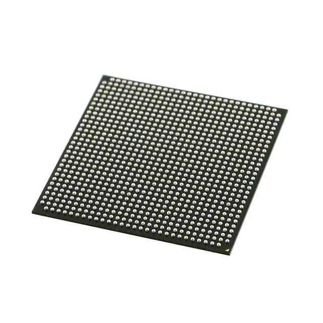
- Package: Flip-chip BGA (Ball Grid Array)
- Essence: FPGA (Field-Programmable Gate Array)
- Packaging/Quantity: Single unit
Specifications
- Technology: 28nm
- Logic Elements: 358,400
- Embedded Memory: 10,368 Kbits
- DSP Blocks: 1,890
- Maximum User I/Os: 1,040
- Operating Voltage: 1.2V
- Speed Grade: -7
Detailed Pin Configuration
The 5CGTFD7D5F31C7N has a total of 1,040 user I/O pins, which are configurable for various purposes such as input, output, or bidirectional communication. The pin configuration is detailed in the datasheet provided by the manufacturer.
Functional Features
- High-performance: The 5CGTFD7D5F31C7N offers fast processing capabilities due to its advanced technology and architecture.
- Low-power: It is designed to consume minimal power, making it suitable for battery-powered devices or energy-efficient applications.
- High-density: With a large number of logic elements and embedded memory, it provides ample resources for complex designs.
- Programmability: The FPGA nature allows users to configure the device according to their specific requirements, enabling flexibility and customization.
Advantages and Disadvantages
Advantages: - Versatility: The programmable nature of the device makes it adaptable to a wide range of applications. - Rapid Prototyping: FPGA-based solutions enable quick development and testing of new designs. - Reconfigurability: Changes can be made to the logic and functionality of the device without requiring hardware modifications.
Disadvantages: - Complexity: Designing for FPGAs can be challenging, requiring expertise in digital design and programming. - Cost: FPGA devices tend to be more expensive compared to fixed-function integrated circuits. - Power Consumption: While efforts have been made to reduce power consumption, FPGAs still consume more power than dedicated ASICs (Application-Specific Integrated Circuits).
Working Principles
The 5CGTFD7D5F31C7N is based on the principle of reconfigurable computing. It consists of an array of programmable logic blocks interconnected by configurable routing resources. The device can be programmed using a Hardware Description Language (HDL) such as VHDL or Verilog. Once programmed, the FPGA implements the desired logic functions and can perform various tasks based on the user's requirements.
Detailed Application Field Plans
The 5CGTFD7D5F31C7N finds applications in various fields, including but not limited to: 1. Communications: Used in wireless base stations, network routers, and switches for high-speed data processing. 2. Industrial Automation: Enables control systems, robotics, and machine vision applications. 3. Automotive: Utilized in advanced driver-assistance systems (ADAS), infotainment systems, and engine control units (ECUs). 4. Aerospace and Defense: Employed in radar systems, avionics, and secure communication systems. 5. Medical: Used in medical imaging devices, patient monitoring systems, and laboratory equipment.
Detailed and Complete Alternative Models
- 5CGXFC9E6F31C7N: Similar to 5CGTFD7D5F31C7N, but with different specifications and features.
- 5CEBA9F23I7N: An alternative FPGA with lower logic elements but higher DSP blocks.
- 5SGXEA7N2F45C2N: Offers higher logic density and more I/O pins compared to 5CGTFD7D5F31C7N.
These alternative models provide options with varying capabilities and resource requirements, allowing designers to choose the most suitable FPGA for their specific application needs.
Note: The content provided above is a sample structure for an encyclopedia entry and may not reflect actual specifications or details of any specific product.
기술 솔루션에 5CGTFD7D5F31C7N 적용과 관련된 10가지 일반적인 질문과 답변을 나열하세요.
Question: What is the maximum operating temperature for 5CGTFD7D5F31C7N?
Answer: The maximum operating temperature for 5CGTFD7D5F31C7N is 100°C.Question: What is the typical power consumption of 5CGTFD7D5F31C7N?
Answer: The typical power consumption of 5CGTFD7D5F31C7N is 6W.Question: What are the available interfaces on 5CGTFD7D5F31C7N?
Answer: 5CGTFD7D5F31C7N features PCIe, Gigabit Ethernet, and DDR3 interfaces.Question: Can 5CGTFD7D5F31C7N support real-time video processing?
Answer: Yes, 5CGTFD7D5F31C7N can support real-time video processing with its high-performance FPGA fabric.Question: What tools are recommended for programming 5CGTFD7D5F31C7N?
Answer: It is recommended to use Intel Quartus Prime software for programming 5CGTFD7D5F31C7N.Question: Does 5CGTFD7D5F31C7N support secure boot and encryption?
Answer: Yes, 5CGTFD7D5F31C7N supports secure boot and encryption for enhanced security.Question: What is the maximum data transfer rate supported by 5CGTFD7D5F31C7N?
Answer: 5CGTFD7D5F31C7N supports a maximum data transfer rate of 10 Gbps.Question: Can 5CGTFD7D5F31C7N be used in industrial automation applications?
Answer: Yes, 5CGTFD7D5F31C7N is suitable for industrial automation applications due to its reliability and performance.Question: Are there any specific design considerations for using 5CGTFD7D5F31C7N in automotive systems?
Answer: When using 5CGTFD7D5F31C7N in automotive systems, it's important to consider temperature range and EMI/EMC requirements.Question: What are the key advantages of using 5CGTFD7D5F31C7N in telecommunications infrastructure?
Answer: 5CGTFD7D5F31C7N offers high-speed processing, low latency, and flexibility, making it ideal for telecommunications infrastructure.