

5CGXFC7D7F27C8N
Product Overview
Category
The 5CGXFC7D7F27C8N belongs to the category of Field Programmable Gate Arrays (FPGAs).
Use
FPGAs are integrated circuits that can be programmed and reprogrammed to perform various digital functions. The 5CGXFC7D7F27C8N is specifically designed for high-performance applications.
Characteristics
- High-performance FPGA with advanced features
- Flexible and reprogrammable design
- Supports complex digital logic functions
- Offers high-speed data processing capabilities
- Suitable for demanding applications requiring real-time processing
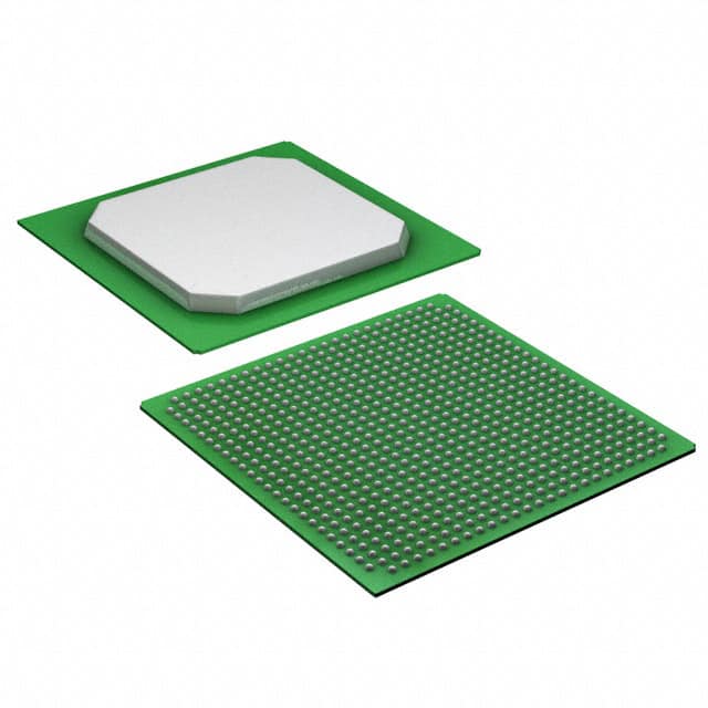
Package
The 5CGXFC7D7F27C8N comes in a compact package, ensuring easy integration into electronic systems.
Essence
The essence of the 5CGXFC7D7F27C8N lies in its ability to provide a customizable and high-performance solution for digital logic applications.
Packaging/Quantity
The 5CGXFC7D7F27C8N is typically packaged individually and is available in various quantities depending on the customer's requirements.
Specifications
- FPGA Family: Cyclone V GX
- Logic Elements: 77,760
- Embedded Memory: 3,888 Kbits
- Maximum User I/Os: 622
- Operating Voltage: 1.2V
- Speed Grade: -8
- Package Type: FBGA
- Package Pins: 780
- Temperature Range: -40°C to +100°C
Detailed Pin Configuration
The detailed pin configuration of the 5CGXFC7D7F27C8N can be found in the manufacturer's datasheet or technical documentation.
Functional Features
- High-speed serial transceivers for fast data communication
- Dedicated digital signal processing (DSP) blocks for efficient mathematical operations
- On-chip memory resources for data storage and retrieval
- Configurable I/O standards for compatibility with various interfaces
- Built-in security features to protect sensitive information
Advantages and Disadvantages
Advantages
- Flexibility: The 5CGXFC7D7F27C8N can be reprogrammed to adapt to changing requirements.
- High Performance: It offers powerful processing capabilities for demanding applications.
- Integration: The compact package allows for easy integration into electronic systems.
Disadvantages
- Complexity: Programming and utilizing FPGAs require specialized knowledge and expertise.
- Cost: FPGAs can be more expensive compared to other integrated circuits for certain applications.
Working Principles
The 5CGXFC7D7F27C8N operates based on the principles of configurable logic. It consists of a matrix of programmable logic elements interconnected by configurable routing resources. These logic elements can be programmed to perform specific functions, allowing the FPGA to execute complex digital operations.
Detailed Application Field Plans
The 5CGXFC7D7F27C8N finds applications in various fields, including: 1. Telecommunications: Used in high-speed data communication systems. 2. Aerospace and Defense: Employed in radar systems, avionics, and secure communications. 3. Industrial Automation: Utilized for real-time control and monitoring in manufacturing processes. 4. Medical Devices: Integrated into medical imaging systems and diagnostic equipment. 5. Research and Development: Used as a prototyping platform for digital designs.
Detailed and Complete Alternative Models
- 5CGXFC7D6F27C8N
- 5CGXFC7D5F27C8N
- 5CGXFC7D4F27C8N
- 5CGXFC7D3F27C8N
These alternative models offer similar features and capabilities, with variations in logic elements, memory, or I/O count.
Note: The content provided above is a sample structure for an encyclopedia entry and does not represent actual specifications or details of the mentioned product.
기술 솔루션에 5CGXFC7D7F27C8N 적용과 관련된 10가지 일반적인 질문과 답변을 나열하세요.
Sure! Here are 10 common questions and answers related to the application of 5CGXFC7D7F27C8N in technical solutions:
Q: What is the 5CGXFC7D7F27C8N? A: The 5CGXFC7D7F27C8N is a field-programmable gate array (FPGA) manufactured by Intel.
Q: What are the key features of the 5CGXFC7D7F27C8N? A: The key features include 27,280 logic elements, 1,288 embedded memory blocks, 6 PLLs, and support for various I/O standards.
Q: What are some typical applications of the 5CGXFC7D7F27C8N? A: The 5CGXFC7D7F27C8N can be used in a wide range of applications such as telecommunications, industrial automation, automotive systems, and high-performance computing.
Q: How can I program the 5CGXFC7D7F27C8N? A: You can program the 5CGXFC7D7F27C8N using Intel's Quartus Prime software, which provides a user-friendly interface for designing and programming FPGAs.
Q: What are the power requirements for the 5CGXFC7D7F27C8N? A: The 5CGXFC7D7F27C8N requires a supply voltage of 1.0V for core logic and 3.3V for I/O banks.
Q: Can I use the 5CGXFC7D7F27C8N in a high-speed data processing system? A: Yes, the 5CGXFC7D7F27C8N is capable of handling high-speed data processing with its embedded memory blocks and support for various I/O standards.
Q: Does the 5CGXFC7D7F27C8N support communication protocols like Ethernet or USB? A: Yes, the 5CGXFC7D7F27C8N supports various communication protocols including Ethernet, USB, PCIe, and more.
Q: Can I use the 5CGXFC7D7F27C8N for real-time signal processing applications? A: Absolutely! The 5CGXFC7D7F27C8N's high logic density and embedded memory make it suitable for real-time signal processing tasks.
Q: Are there any development boards available for the 5CGXFC7D7F27C8N? A: Yes, Intel offers development boards specifically designed for the 5CGXFC7D7F27C8N, which provide a convenient platform for prototyping and testing.
Q: Where can I find technical documentation and support for the 5CGXFC7D7F27C8N? A: You can find technical documentation, application notes, and support resources on Intel's website or by contacting their customer support team.
Please note that the specific details and answers may vary depending on the manufacturer's documentation and specifications.