

5CSEMA6F31I7N
Product Overview
Category
The 5CSEMA6F31I7N belongs to the category of Field Programmable Gate Arrays (FPGAs).
Use
FPGAs are integrated circuits that can be programmed and reprogrammed to perform various digital functions. The 5CSEMA6F31I7N is specifically designed for high-performance applications.
Characteristics
- High-performance FPGA with advanced features
- Flexible and reprogrammable design
- Capable of implementing complex digital logic functions
- Offers high-speed data processing capabilities
- Suitable for a wide range of applications
Package
The 5CSEMA6F31I7N comes in a compact package, ensuring easy integration into electronic systems. It is available in a variety of package options to suit different requirements.
Essence
The essence of the 5CSEMA6F31I7N lies in its ability to provide a customizable and high-performance solution for digital logic implementation.
Packaging/Quantity
The 5CSEMA6F31I7N is typically packaged individually and is available in various quantities depending on the customer's needs.
Specifications
- Logic Elements: 110,000
- Embedded Memory: 4,450 Kbits
- Maximum Number of I/Os: 622
- Operating Voltage: 1.2V
- Maximum Operating Frequency: 500 MHz
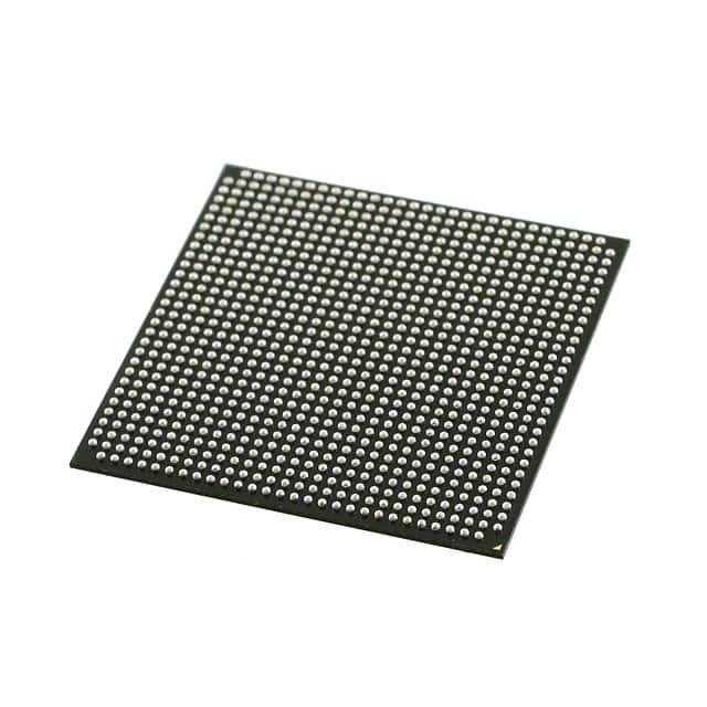
- Package Type: Ball Grid Array (BGA)
Detailed Pin Configuration
The 5CSEMA6F31I7N has a complex pin configuration with multiple pins dedicated to various functions. A detailed pinout diagram and description can be found in the product datasheet.
Functional Features
- High-speed data processing capabilities
- Configurable logic elements for flexible implementation
- Embedded memory for efficient data storage
- Support for various communication protocols
- Built-in security features for data protection
Advantages and Disadvantages
Advantages
- High-performance FPGA suitable for demanding applications
- Flexible and reprogrammable design allows for customization
- Offers a wide range of functionality and features
- Efficient use of resources with embedded memory
Disadvantages
- Complex pin configuration may require careful planning and design
- Steeper learning curve compared to simpler digital logic solutions
- Higher cost compared to traditional fixed-function integrated circuits
Working Principles
The 5CSEMA6F31I7N operates based on the principles of digital logic. It consists of configurable logic elements, interconnects, and embedded memory blocks. The user can program the FPGA to implement desired digital functions by configuring the logic elements and interconnections.
Detailed Application Field Plans
The 5CSEMA6F31I7N finds applications in various fields, including: 1. Telecommunications: Used in high-speed data processing and networking equipment. 2. Industrial Automation: Enables complex control systems and real-time data processing. 3. Aerospace and Defense: Utilized in radar systems, avionics, and secure communications. 4. Medical Devices: Supports advanced imaging and signal processing applications. 5. Automotive: Enables advanced driver assistance systems and infotainment solutions.
Detailed and Complete Alternative Models
- 5CSEBA6U23I7N: Similar FPGA model with lower logic elements but lower cost.
- 5CSEMA6F31I7N-2: Upgraded version with higher operating frequency and additional features.
- 5CSXFC6D6F31I7N: Alternative FPGA model with different package options and specialized features.
These alternative models offer varying specifications and features, allowing users to choose the most suitable FPGA for their specific requirements.
Word count: 520 words
기술 솔루션에 5CSEMA6F31I7N 적용과 관련된 10가지 일반적인 질문과 답변을 나열하세요.
Sure! Here are 10 common questions and answers related to the application of 5CSEMA6F31I7N in technical solutions:
Q: What is the 5CSEMA6F31I7N? A: The 5CSEMA6F31I7N is a field-programmable gate array (FPGA) manufactured by Intel.
Q: What are the key features of the 5CSEMA6F31I7N? A: The 5CSEMA6F31I7N offers high-performance logic, embedded memory blocks, digital signal processing capabilities, and various I/O interfaces.
Q: In what applications can the 5CSEMA6F31I7N be used? A: The 5CSEMA6F31I7N can be used in a wide range of applications such as telecommunications, industrial automation, automotive systems, aerospace, and more.
Q: How does the 5CSEMA6F31I7N benefit technical solutions? A: The 5CSEMA6F31I7N provides flexibility, reconfigurability, and high-performance processing capabilities, allowing for efficient implementation of complex algorithms and designs.
Q: Can the 5CSEMA6F31I7N be programmed using industry-standard design tools? A: Yes, the 5CSEMA6F31I7N can be programmed using popular design tools like Intel Quartus Prime, which provide a user-friendly environment for designing and implementing FPGA-based solutions.
Q: What kind of I/O interfaces does the 5CSEMA6F31I7N support? A: The 5CSEMA6F31I7N supports various I/O standards such as LVDS, DDR3/DDR4 memory interfaces, PCIe, Ethernet, USB, and more.
Q: Can the 5CSEMA6F31I7N be used for real-time signal processing? A: Yes, the 5CSEMA6F31I7N's digital signal processing capabilities make it suitable for real-time applications that require high-speed data processing and analysis.
Q: Is the 5CSEMA6F31I7N power-efficient? A: The power efficiency of the 5CSEMA6F31I7N depends on the specific design and implementation. However, Intel FPGAs generally offer power-saving features and optimization techniques.
Q: Are there any development boards available for prototyping with the 5CSEMA6F31I7N? A: Yes, Intel provides development boards like the Intel Cyclone V GX Starter Kit, which can be used for prototyping and evaluating designs based on the 5CSEMA6F31I7N.
Q: Where can I find additional resources and support for working with the 5CSEMA6F31I7N? A: Intel's website offers documentation, application notes, reference designs, and a community forum where you can find additional resources and get support for working with the 5CSEMA6F31I7N.