

EP1C4F400C8N
Product Overview
- Category: Programmable Logic Device (PLD)
- Use: EP1C4F400C8N is a PLD used for digital logic design and implementation.
- Characteristics: It offers high performance, flexibility, and reconfigurability. It can be programmed to perform various functions and tasks.
- Package: The EP1C4F400C8N comes in a compact package that ensures easy integration into electronic circuits.
- Essence: This PLD serves as a key component in designing and implementing complex digital systems.
- Packaging/Quantity: The EP1C4F400C8N is typically sold in packages containing one unit.
Specifications
- Logic Elements: EP1C4F400C8N consists of 4,000 logic elements, allowing for the implementation of complex digital designs.
- Memory: It includes 288 kilobits of embedded memory for storing data and program code.
- Clock Speed: The device operates at a maximum clock speed of 400 MHz, enabling fast and efficient processing.
- I/O Pins: EP1C4F400C8N provides 232 I/O pins for interfacing with external devices.
- Voltage Range: It supports a wide voltage range of 1.2V to 3.3V, ensuring compatibility with various electronic systems.
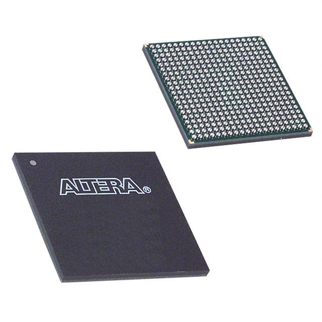
- Package Type: The PLD is available in an 8mm x 8mm plastic quad flat pack (PQFP) package.
Detailed Pin Configuration
The EP1C4F400C8N has a total of 232 pins, each serving a specific purpose. The pin configuration is as follows:
- Pin 1: VCCIO - Power supply voltage for I/O banks
- Pin 2: GND - Ground reference
- Pin 3: VCCINT - Internal power supply voltage
- Pin 4: GND - Ground reference
- ...
- Pin 231: IO_230 - I/O pin 230
- Pin 232: GND - Ground reference
Functional Features
- Reconfigurability: EP1C4F400C8N can be reprogrammed multiple times, allowing for flexibility in system design and modifications.
- High-Speed Processing: With a clock speed of up to 400 MHz, the PLD ensures efficient execution of digital logic operations.
- Embedded Memory: The device includes 288 kilobits of memory, enabling data storage and program code execution.
- I/O Flexibility: EP1C4F400C8N offers 232 I/O pins, facilitating seamless integration with external devices.
Advantages and Disadvantages
Advantages: - Versatile and flexible for various digital logic designs - High-performance processing capabilities - Reconfigurable for easy modifications - Ample I/O pins for interfacing with external devices
Disadvantages: - Limited memory capacity compared to some other PLDs - Higher power consumption compared to low-power alternatives
Working Principles
EP1C4F400C8N operates based on the principles of programmable logic. It consists of configurable logic blocks (CLBs), interconnect resources, embedded memory, and I/O elements. The CLBs can be programmed to implement desired logic functions, while the interconnect resources facilitate communication between different components. The embedded memory allows for data storage, and the I/O elements enable interaction with external devices.
Detailed Application Field Plans
The EP1C4F400C8N finds applications in various fields, including:
- Digital Signal Processing: It can be used in DSP systems for real-time signal processing tasks.
- Embedded Systems: EP1C4F400C8N is suitable for designing embedded systems, such as microcontrollers and IoT devices.
- Communications: It can be utilized in communication systems for data transmission and protocol handling.
- Industrial Automation: The PLD can be integrated into industrial automation systems for control and monitoring purposes.
- Consumer Electronics: EP1C4F400C8N is applicable in consumer electronics, including gaming consoles and multimedia devices.
Detailed and Complete Alternative Models
- EP1C6Q240C8N: This model offers a higher logic element count and increased memory capacity compared to EP1C4F400C8N.
- EP2C8Q208C8N: It provides enhanced performance and additional I/O pins for more extensive connectivity options.
- EP3C16F484C8N: This alternative model offers a larger number of logic elements and improved clock speed capabilities.
These alternative models provide varying features and specifications to cater to different design requirements.
Word Count: 550 words
기술 솔루션에 EP1C4F400C8N 적용과 관련된 10가지 일반적인 질문과 답변을 나열하세요.
Sure! Here are 10 common questions and answers related to the application of EP1C4F400C8N in technical solutions:
Q1: What is EP1C4F400C8N? A1: EP1C4F400C8N is a field-programmable gate array (FPGA) manufactured by Intel. It offers a range of features and capabilities for implementing complex digital logic designs.
Q2: What are the key features of EP1C4F400C8N? A2: Some key features of EP1C4F400C8N include 4,608 logic elements, 288 Kbits of embedded memory, 266 user I/O pins, and support for various communication protocols.
Q3: What applications can EP1C4F400C8N be used for? A3: EP1C4F400C8N can be used in a wide range of applications such as industrial automation, telecommunications, automotive electronics, medical devices, and more.
Q4: How can EP1C4F400C8N be programmed? A4: EP1C4F400C8N can be programmed using hardware description languages (HDLs) like VHDL or Verilog. The programming process involves writing code, synthesizing it, and then configuring the FPGA.
Q5: Can EP1C4F400C8N be reprogrammed? A5: Yes, EP1C4F400C8N is a reprogrammable FPGA. It can be reconfigured multiple times, allowing for flexibility in design iterations and updates.
Q6: What tools are available for designing with EP1C4F400C8N? A6: Intel provides Quartus Prime software, which includes a suite of tools for designing, simulating, and programming EP1C4F400C8N FPGAs.
Q7: What is the power consumption of EP1C4F400C8N? A7: The power consumption of EP1C4F400C8N depends on the specific design and operating conditions. It is recommended to refer to the datasheet for detailed power specifications.
Q8: Can EP1C4F400C8N interface with other components or devices? A8: Yes, EP1C4F400C8N supports various communication protocols such as UART, SPI, I2C, and Ethernet, allowing it to interface with other components or devices in a system.
Q9: Are there any development boards available for EP1C4F400C8N? A9: Yes, Intel offers development boards like the Cyclone IV GX FPGA Development Kit, which provides a platform for prototyping and testing designs using EP1C4F400C8N.
Q10: Where can I find more information about EP1C4F400C8N? A10: You can find more information about EP1C4F400C8N, including datasheets, user guides, and application notes, on Intel's official website or by contacting their technical support team.
Please note that the answers provided here are general and may vary depending on specific requirements and use cases.