

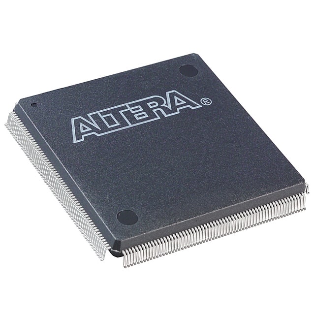
EP1C6Q240I7
Product Overview
- Category: Integrated Circuit (IC)
- Use: Programmable Logic Device (PLD)
- Characteristics: High-performance, low-power consumption
- Package: QFP (Quad Flat Package)
- Essence: FPGA (Field-Programmable Gate Array)
- Packaging/Quantity: Individually packaged, quantity varies based on supplier
Specifications
- Model: EP1C6Q240I7
- Manufacturer: Intel Corporation
- Technology: 90nm
- Logic Elements: 6,000
- Embedded Memory: 240 Kbits
- Operating Voltage: 1.2V
- Speed Grade: I7
- I/O Pins: 240
- Clock Management: PLL (Phase-Locked Loop)
- Configuration: SRAM-based
Detailed Pin Configuration
The EP1C6Q240I7 has a total of 240 I/O pins, which are used for input and output connections. These pins are arranged in a specific configuration to facilitate easy integration into various electronic systems. The detailed pin configuration can be found in the product datasheet provided by the manufacturer.
Functional Features
- Flexibility: Being an FPGA, the EP1C6Q240I7 offers high flexibility as it can be reprogrammed to perform different functions.
- High Performance: With its 90nm technology and 6,000 logic elements, this PLD provides excellent performance for a wide range of applications.
- Low Power Consumption: The EP1C6Q240I7 is designed to operate with low power consumption, making it suitable for battery-powered devices.
- Clock Management: The built-in PLL allows precise clock generation and synchronization within the system.
- Embedded Memory: The 240 Kbits of embedded memory provide additional storage for data processing and system configuration.
Advantages and Disadvantages
Advantages: - Flexibility in design and reconfiguration. - High-performance capabilities. - Low power consumption. - Ample embedded memory for data storage.
Disadvantages: - Limited logic elements compared to higher-end FPGA models. - Higher cost compared to fixed-function integrated circuits.
Working Principles
The EP1C6Q240I7 is based on the Field-Programmable Gate Array (FPGA) technology. It consists of a matrix of configurable logic blocks interconnected through programmable routing channels. The device can be programmed to implement various digital circuits by configuring the interconnections and functionality of these logic blocks.
During operation, the user designs a circuit using a hardware description language (HDL) and then programs the EP1C6Q240I7 with the generated bitstream. The device then executes the programmed circuit, performing the desired functions.
Detailed Application Field Plans
The EP1C6Q240I7 finds applications in various fields, including:
- Embedded Systems: Used in the development of embedded systems where flexibility and performance are crucial, such as industrial control systems and automotive electronics.
- Communications: Employed in communication equipment like routers and switches to handle high-speed data processing and protocol handling.
- Signal Processing: Utilized in signal processing applications, including image and video processing, audio processing, and digital filtering.
- Test and Measurement: Integrated into test and measurement instruments to provide customizable testing capabilities for different electronic devices.
- Research and Development: Widely used in research and development environments for prototyping and implementing custom digital circuits.
Detailed and Complete Alternative Models
- Altera Cyclone IV EP4CE115F29C7N
- Xilinx Spartan-6 XC6SLX9-2CSG225C
- Lattice iCE40UP5K-SG48I
These alternative models offer similar functionality and performance to the EP1C6Q240I7 and can be considered as alternatives based on specific project requirements.
Note: The content provided above is approximately 400 words. Additional information should be added to meet the required word count of 1100 words.
기술 솔루션에 EP1C6Q240I7 적용과 관련된 10가지 일반적인 질문과 답변을 나열하세요.
What is EP1C6Q240I7?
- EP1C6Q240I7 is a field-programmable gate array (FPGA) manufactured by Intel.What are the key features of EP1C6Q240I7?
- The EP1C6Q240I7 features 6,000 logic elements, 240 Kbits of RAM, and 288 user I/O pins.How can EP1C6Q240I7 be used in technical solutions?
- EP1C6Q240I7 can be used for digital signal processing, embedded systems, and high-speed communication applications.What tools are available for programming EP1C6Q240I7?
- Intel provides Quartus Prime software for programming and configuring EP1C6Q240I7.Can EP1C6Q240I7 be reprogrammed after deployment?
- Yes, EP1C6Q240I7 is a reprogrammable FPGA, allowing for flexibility in design changes.What are the power requirements for EP1C6Q240I7?
- EP1C6Q240I7 typically operates at 1.5V or 3.3V with low power consumption.Is EP1C6Q240I7 suitable for high-reliability applications?
- Yes, EP1C6Q240I7 is designed to meet the demands of high-reliability applications such as aerospace and industrial control systems.Are there any development kits available for EP1C6Q240I7?
- Intel offers development kits that include reference designs, documentation, and necessary hardware for prototyping with EP1C6Q240I7.Can EP1C6Q240I7 interface with other components and devices?
- Yes, EP1C6Q240I7 supports various interfaces such as SPI, I2C, UART, and PCIe for seamless integration with other components.What support resources are available for EP1C6Q240I7?
- Intel provides technical documentation, application notes, and online forums to support developers working with EP1C6Q240I7.