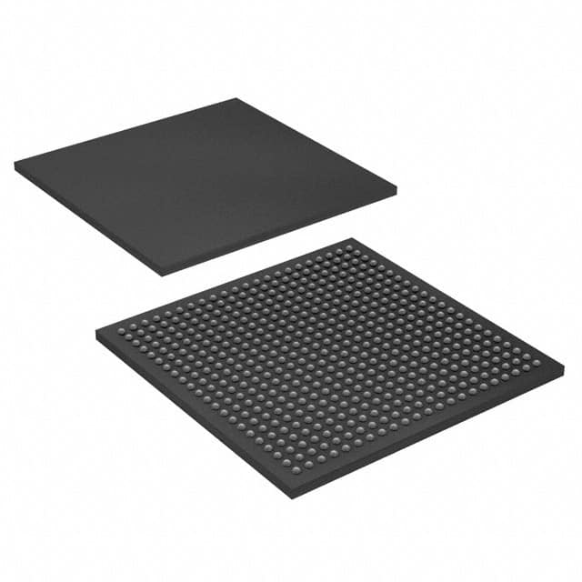
EP1K50FC484-2N
Product Overview
Category: Integrated Circuit (IC)
Use: The EP1K50FC484-2N is a programmable logic device (PLD) that belongs to the family of Field-Programmable Gate Arrays (FPGAs). It is designed for use in various digital applications, including telecommunications, industrial automation, consumer electronics, and more.
Characteristics: - High-performance FPGA with 1,536 logic elements - 50,000 usable gates - 3.3V core voltage - 484-pin FineLine BGA package - Flash memory technology for reprogramming flexibility
Package and Quantity: The EP1K50FC484-2N is available in a FineLine BGA package, which consists of a 484-pin chip. It is typically sold individually or in small quantities.
Essence: This PLD offers a versatile and flexible solution for implementing complex digital circuits. Its programmable nature allows users to configure the device according to their specific requirements, eliminating the need for custom-designed integrated circuits.
Packaging/Quantity: The EP1K50FC484-2N is packaged in a FineLine BGA package and is usually sold individually or in small quantities.
Specifications
- Logic Elements: 1,536
- Usable Gates: 50,000
- Core Voltage: 3.3V
- Package Type: FineLine BGA
- Pin Count: 484
Detailed Pin Configuration
The EP1K50FC484-2N has a total of 484 pins, each serving a specific function within the device. The pin configuration varies depending on the specific application and user requirements. For detailed pin assignments and functions, please refer to the manufacturer's datasheet.
Functional Features
- High-density programmable logic device
- Flash memory technology for easy reprogramming
- Flexible and configurable architecture
- Support for various I/O standards
- On-chip clock management circuitry
- Built-in memory blocks for efficient data storage
Advantages and Disadvantages
Advantages: - Versatile and flexible design - Eliminates the need for custom-designed integrated circuits - Reprogrammable for easy updates and modifications - High-performance capabilities - Support for various I/O standards
Disadvantages: - Limited gate count compared to larger FPGAs - Higher power consumption compared to dedicated ASICs - Requires specialized knowledge for programming and configuration
Working Principles
The EP1K50FC484-2N operates based on the principles of field-programmable gate arrays. It consists of a matrix of programmable logic elements that can be interconnected to create complex digital circuits. The device is programmed using hardware description languages (HDL) or graphical tools, which define the desired functionality and interconnections within the FPGA.
Once programmed, the EP1K50FC484-2N executes the specified logic operations, allowing it to perform various tasks such as data processing, signal routing, and control functions. The device utilizes flash memory technology, enabling users to reprogram it multiple times to accommodate changing requirements.
Detailed Application Field Plans
The EP1K50FC484-2N finds applications in a wide range of industries and fields, including:
- Telecommunications: Used in network routers, switches, and communication equipment for data processing and protocol handling.
- Industrial Automation: Employed in programmable logic controllers (PLCs), motor control systems, and industrial monitoring devices for process control and automation.
- Consumer Electronics: Integrated into smart TVs, set-top boxes, gaming consoles, and audio/video equipment for signal processing and control functions.
- Automotive: Utilized in automotive electronics for engine control units (ECUs), advanced driver-assistance systems (ADAS), and infotainment systems.
- Aerospace and Defense: Deployed in avionics, radar systems, and military communication equipment for high-performance digital signal processing and data handling.
Detailed and Complete Alternative Models
- EP2C20F484C7N: A similar FPGA with 2,016 logic elements and 20,000 usable gates. It features a 3.3V core voltage and is packaged in a 484-pin FineLine BGA package.
- XC6SLX9-2FTG256C: Another FPGA option with 6,080 logic cells and 9,152 slices. It operates at a 1.2V core voltage and comes in a 256-pin Thin Fine-Pitch Ball Grid Array (TFBGA) package.
- MAX 10M08SAE144C8G: An alternative FPGA with 8,000 logic elements and 10,570 adaptive lookup tables (ALUTs). It supports a 1.8V core voltage and is available in a 144-pin Enhanced
기술 솔루션에 EP1K50FC484-2N 적용과 관련된 10가지 일반적인 질문과 답변을 나열하세요.
Sure! Here are 10 common questions and answers related to the application of EP1K50FC484-2N in technical solutions:
Q1: What is EP1K50FC484-2N? A1: EP1K50FC484-2N is a field-programmable gate array (FPGA) manufactured by Intel. It is designed for various applications in digital logic circuits.
Q2: What are the key features of EP1K50FC484-2N? A2: Some key features of EP1K50FC484-2N include 50,000 logic elements, 3.3V operation, 484-pin package, and support for various I/O standards.
Q3: What are the typical applications of EP1K50FC484-2N? A3: EP1K50FC484-2N can be used in a wide range of applications such as telecommunications, industrial automation, medical devices, automotive systems, and aerospace.
Q4: How can EP1K50FC484-2N be programmed? A4: EP1K50FC484-2N can be programmed using hardware description languages (HDLs) like VHDL or Verilog, which allow designers to describe the desired functionality of the FPGA.
Q5: Can EP1K50FC484-2N be reprogrammed after deployment? A5: Yes, EP1K50FC484-2N is a reprogrammable FPGA, meaning it can be reconfigured with new designs even after it has been deployed in a system.
Q6: What tools are available for designing with EP1K50FC484-2N? A6: Intel provides Quartus Prime software, which includes design entry, synthesis, simulation, and programming tools specifically tailored for working with their FPGAs.
Q7: What is the power consumption of EP1K50FC484-2N? A7: The power consumption of EP1K50FC484-2N depends on the specific design and operating conditions. It is recommended to refer to the datasheet for detailed power specifications.
Q8: Can EP1K50FC484-2N interface with other components or devices? A8: Yes, EP1K50FC484-2N supports various I/O standards, allowing it to interface with a wide range of components and devices such as sensors, memory, communication interfaces, and more.
Q9: Are there any limitations or constraints when using EP1K50FC484-2N? A9: EP1K50FC484-2N has certain limitations like finite resources (logic elements, memory blocks), limited I/O pins, and specific timing requirements that need to be considered during design.
Q10: Where can I find additional resources and support for EP1K50FC484-2N? A10: Intel provides documentation, application notes, reference designs, and a community forum where users can find additional resources and get support for EP1K50FC484-2N.


