

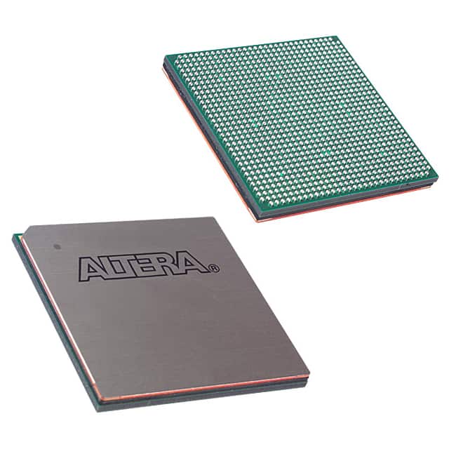
EP1S25F1020C6N
Product Overview
Category
The EP1S25F1020C6N belongs to the category of Field Programmable Gate Arrays (FPGAs).
Use
FPGAs are integrated circuits that can be programmed and reprogrammed to perform various digital functions. The EP1S25F1020C6N is specifically designed for high-performance applications.
Characteristics
- High-performance FPGA with advanced features
- Programmable logic cells for flexible design implementation
- Large number of I/O pins for connectivity
- High-speed interfaces for data transfer
- Low power consumption for energy efficiency
Package
The EP1S25F1020C6N comes in a compact package, suitable for surface mount technology (SMT) assembly.
Essence
The essence of the EP1S25F1020C6N lies in its ability to provide a customizable hardware solution for complex digital systems.
Packaging/Quantity
The EP1S25F1020C6N is typically packaged in reels or trays, with a quantity of 100 units per package.
Specifications
- Logic Elements: 25,000
- Embedded Memory: 1,020 Kbits
- Maximum User I/O Pins: 500
- Clock Management: Phase-Locked Loops (PLLs)
- Operating Voltage: 1.2V
- Operating Temperature Range: -40°C to 100°C
- Package Type: FBGA (Fine-Pitch Ball Grid Array)
Detailed Pin Configuration
The EP1S25F1020C6N has a comprehensive pin configuration, allowing for versatile connectivity and integration within a system. The detailed pin configuration can be found in the product datasheet.
Functional Features
High-Speed Interfaces
The EP1S25F1020C6N supports various high-speed interfaces, such as DDR3 memory interfaces and PCIe (Peripheral Component Interconnect Express) for fast data transfer.
Programmable Logic Cells
With 25,000 logic elements, the EP1S25F1020C6N offers a large number of programmable logic cells, enabling designers to implement complex digital functions efficiently.
Clock Management
The built-in Phase-Locked Loops (PLLs) provide precise clock management capabilities, allowing for synchronization and timing control in the FPGA design.
Advantages and Disadvantages
Advantages
- High-performance FPGA suitable for demanding applications
- Flexible and customizable design implementation
- Extensive I/O connectivity options
- Low power consumption for energy-efficient operation
Disadvantages
- Relatively higher cost compared to other programmable logic devices
- Steeper learning curve for inexperienced users due to complexity
Working Principles
The EP1S25F1020C6N operates based on the principles of reconfigurable hardware. It consists of an array of programmable logic cells interconnected through configurable routing resources. The user can program the FPGA to define the desired functionality by configuring the interconnections and logic within the device.
Detailed Application Field Plans
The EP1S25F1020C6N finds applications in various fields, including: - Telecommunications - Data centers - Industrial automation - Aerospace and defense - Medical equipment - Automotive electronics
Detailed and Complete Alternative Models
- EP2S60F1020C5N: A higher-capacity FPGA with 60,000 logic elements
- EP4CE115F29C7N: A lower-cost FPGA with 115,000 logic elements
- EP1C20F324I7N: A compact FPGA with 20,000 logic elements and extended temperature range
These alternative models offer different capacities and features to cater to diverse design requirements.
Word count: 515 words
기술 솔루션에 EP1S25F1020C6N 적용과 관련된 10가지 일반적인 질문과 답변을 나열하세요.
Sure! Here are 10 common questions and answers related to the application of EP1S25F1020C6N in technical solutions:
Q1: What is EP1S25F1020C6N? A1: EP1S25F1020C6N is a specific model of Field Programmable Gate Array (FPGA) manufactured by Intel.
Q2: What are the key features of EP1S25F1020C6N? A2: Some key features of EP1S25F1020C6N include 25,000 logic elements, 1,020 Kbits of embedded memory, and support for various I/O standards.
Q3: What are the typical applications of EP1S25F1020C6N? A3: EP1S25F1020C6N is commonly used in applications such as industrial automation, telecommunications, automotive electronics, and high-performance computing.
Q4: How can EP1S25F1020C6N be programmed? A4: EP1S25F1020C6N can be programmed using hardware description languages (HDLs) like VHDL or Verilog, along with design software provided by Intel.
Q5: Can EP1S25F1020C6N be reprogrammed after initial programming? A5: Yes, EP1S25F1020C6N is a reprogrammable FPGA, allowing for flexibility in design iterations and updates.
Q6: What are the power requirements for EP1S25F1020C6N? A6: EP1S25F1020C6N typically operates at a voltage range of 1.2V to 3.3V, depending on the specific design requirements.
Q7: Does EP1S25F1020C6N support high-speed interfaces? A7: Yes, EP1S25F1020C6N supports various high-speed interfaces such as PCIe, DDR3/4 memory interfaces, and Ethernet.
Q8: Can EP1S25F1020C6N interface with external devices? A8: Yes, EP1S25F1020C6N has multiple I/O pins that can be used to interface with external devices such as sensors, displays, or communication modules.
Q9: Are there any development boards available for EP1S25F1020C6N? A9: Yes, Intel provides development boards specifically designed for EP1S25F1020C6N, which include necessary connectors and peripherals for prototyping and testing.
Q10: Where can I find technical documentation and support for EP1S25F1020C6N? A10: Technical documentation, datasheets, and support resources for EP1S25F1020C6N can be found on Intel's official website or by contacting their customer support.