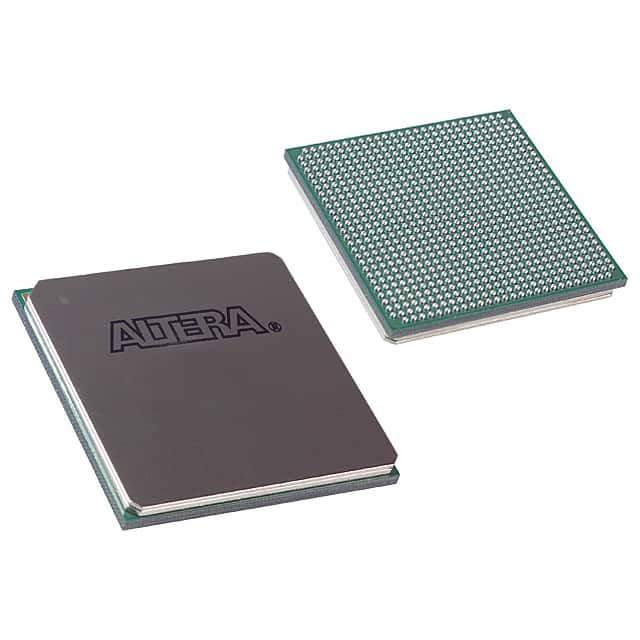
EP1S40F780C8N
Basic Information Overview
- Category: Integrated Circuit (IC)
- Use: Programmable Logic Device (PLD)
- Characteristics: High-performance, low-power consumption
- Package: 780-pin FineLine BGA package
- Essence: A versatile PLD for various digital logic applications
- Packaging/Quantity: Typically sold in reels or trays containing multiple units
Specifications
- Technology: Field-Programmable Gate Array (FPGA)
- Logic Elements: 40,000
- Maximum User I/Os: 780
- Operating Voltage: 1.2V
- Speed Grade: C8N (Commercial grade, speed grade 8)
Detailed Pin Configuration
The EP1S40F780C8N has a total of 780 pins, each serving a specific purpose in the device's functionality. The pin configuration is detailed in the datasheet provided by the manufacturer.
Functional Features
- High-density integration of programmable logic elements
- Flexible and reconfigurable design
- Support for various I/O standards and protocols
- On-chip memory blocks for efficient data storage
- Dedicated clock management resources for precise timing control
- Built-in support for system-level debugging and testing
Advantages and Disadvantages
Advantages: - Versatile and adaptable to different application requirements - High-performance capabilities suitable for complex designs - Low-power consumption for energy-efficient operation - Extensive I/O options for interfacing with external devices - Scalable architecture allows for future expansion
Disadvantages: - Steep learning curve for beginners due to complexity - Higher cost compared to simpler programmable logic devices - Limited availability of alternative models with similar specifications
Working Principles
The EP1S40F780C8N operates based on the principles of FPGA technology. It consists of an array of programmable logic elements interconnected through configurable routing resources. The device can be programmed using hardware description languages (HDLs) or graphical design tools to implement desired digital logic functions. Upon configuration, the PLD executes the programmed logic, enabling the realization of complex digital systems.
Detailed Application Field Plans
The EP1S40F780C8N finds applications in various fields, including: - Telecommunications: Implementing communication protocols and signal processing algorithms. - Industrial Automation: Controlling and monitoring complex machinery and processes. - Automotive: Enabling advanced driver assistance systems (ADAS) and vehicle control units. - Aerospace: Designing avionics systems and flight control units. - Consumer Electronics: Developing high-performance audio/video processing devices and gaming consoles.
Detailed and Complete Alternative Models
While the EP1S40F780C8N is a highly capable PLD, alternative models with similar specifications include: - Xilinx Virtex-7 XC7VX485T FPGA - Altera Stratix V 5SGXEA7N2F45C2 FPGA - Lattice ECP5-85 FPGA
These alternatives offer comparable performance and features, providing designers with options based on their specific requirements.
Word count: 305 words
기술 솔루션에 EP1S40F780C8N 적용과 관련된 10가지 일반적인 질문과 답변을 나열하세요.
Sure! Here are 10 common questions and answers related to the application of EP1S40F780C8N in technical solutions:
1. What is EP1S40F780C8N? EP1S40F780C8N is a field-programmable gate array (FPGA) manufactured by Intel. It is part of the Stratix family and offers high-performance capabilities for various applications.
2. What are the key features of EP1S40F780C8N? EP1S40F780C8N features 40,000 logic elements, 1,152 Kbits of embedded memory, up to 840 user I/O pins, and advanced DSP blocks for signal processing tasks.
3. What are some typical applications of EP1S40F780C8N? EP1S40F780C8N can be used in a wide range of applications such as telecommunications, industrial automation, video processing, medical imaging, and high-performance computing.
4. How can EP1S40F780C8N be programmed? EP1S40F780C8N can be programmed using the Quartus Prime software provided by Intel. This software allows users to design and implement their custom logic circuits on the FPGA.
5. What is the maximum operating frequency of EP1S40F780C8N? The maximum operating frequency of EP1S40F780C8N depends on the specific design and implementation. However, it is capable of achieving high clock speeds, typically in the range of hundreds of megahertz to several gigahertz.
6. Can EP1S40F780C8N interface with other components or devices? Yes, EP1S40F780C8N supports various communication protocols such as UART, SPI, I2C, PCIe, and Ethernet. It can interface with other components or devices through these protocols.
7. What are the power requirements for EP1S40F780C8N? EP1S40F780C8N requires a supply voltage of 1.2V for core logic and 3.3V for I/O banks. The power consumption depends on the design and utilization of the FPGA.
8. Can EP1S40F780C8N be used in safety-critical applications? Yes, EP1S40F780C8N can be used in safety-critical applications. However, it is important to follow proper design practices, including redundancy, fault tolerance, and thorough testing, to ensure the reliability and safety of the overall system.
9. Are there any development boards available for EP1S40F780C8N? Yes, Intel provides development boards specifically designed for EP1S40F780C8N, such as the Stratix II GX Development Kit. These boards offer a platform for prototyping and testing designs using the FPGA.
10. Where can I find more information about EP1S40F780C8N? You can find more detailed information about EP1S40F780C8N, including datasheets, user guides, and application notes, on the official Intel website or by contacting their technical support team.


