

EP2C5Q208C7
Product Overview
Category: Integrated Circuit (IC)
Use: EP2C5Q208C7 is a programmable logic device (PLD) that belongs to the Cyclone II family of field-programmable gate arrays (FPGAs). It is designed for various applications in digital logic design, including but not limited to embedded systems, telecommunications, industrial automation, and consumer electronics.
Characteristics: - High-performance FPGA with low power consumption - 5,136 logic elements (LEs) - 270 Kbits of embedded memory - 4 phase-locked loops (PLLs) - Support for various I/O standards - Built-in configuration flash memory - On-chip analog-to-digital converters (ADCs) - Flexible and reprogrammable architecture
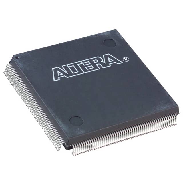
Package: The EP2C5Q208C7 is available in a 208-pin quad flat pack (QFP) package. This package provides ease of soldering and allows for efficient heat dissipation.
Essence: EP2C5Q208C7 is a key component in digital circuit design, enabling designers to implement complex logic functions and algorithms in a single integrated circuit.
Packaging/Quantity: The EP2C5Q208C7 is typically sold individually or in reels, with each reel containing a specific quantity of ICs. The exact packaging and quantity may vary depending on the supplier.
Specifications
- Logic Elements (LEs): 5,136
- Embedded Memory: 270 Kbits
- PLLs: 4
- I/O Standards: Various (TTL, LVCMOS, LVTTL, etc.)
- Configuration Flash Memory: Built-in
- ADC Resolution: Varies (depending on specific model)
- Operating Voltage: 1.2V
- Operating Temperature Range: -40°C to 100°C
- Package Type: 208-pin QFP
Detailed Pin Configuration
The EP2C5Q208C7 has a total of 208 pins, each serving a specific purpose in the overall functionality of the device. The pin configuration may vary depending on the specific model and package variant. For detailed pin assignments and functions, refer to the manufacturer's datasheet or user manual.
Functional Features
- High Logic Capacity: With 5,136 logic elements, the EP2C5Q208C7 provides ample resources for implementing complex digital designs.
- Flexible I/O Support: The device supports various I/O standards, allowing seamless integration with different external devices and interfaces.
- Embedded Memory: The 270 Kbits of embedded memory enables efficient storage and retrieval of data within the FPGA itself.
- On-Chip Analog-to-Digital Converters: The built-in ADCs simplify the integration of analog signals into digital designs.
- Reprogrammable Architecture: The EP2C5Q208C7 can be reprogrammed multiple times, allowing for iterative design improvements and flexibility in adapting to changing requirements.
Advantages and Disadvantages
Advantages: - High logic capacity enables the implementation of complex designs. - Low power consumption makes it suitable for battery-powered applications. - Flexible I/O support allows for easy interfacing with external devices. - On-chip analog-to-digital converters simplify mixed-signal designs. - Reprogrammable architecture offers flexibility and adaptability.
Disadvantages: - Limited number of logic elements compared to higher-end FPGAs. - May require additional external components for certain applications. - Higher cost compared to simpler programmable logic devices.
Working Principles
The EP2C5Q208C7 is based on a field-programmable gate array (FPGA) architecture. It consists of an array of configurable logic elements (LEs) interconnected through programmable routing resources. The LEs can be configured to implement various digital logic functions, such as combinational and sequential circuits.
The device is programmed using a hardware description language (HDL) or a graphical design tool provided by the manufacturer. The programming file is then loaded into the FPGA's configuration flash memory, which determines the behavior and functionality of the circuit implemented within the FPGA.
During operation, the EP2C5Q208C7 executes the programmed logic functions in real-time, responding to input signals and producing the desired output signals based on the defined logic equations and algorithms.
Detailed Application Field Plans
The EP2C5Q208C7 finds applications in a wide range of fields, including:
- Embedded Systems: The FPGA's reprogrammable nature makes it ideal for embedded systems, where flexibility and adaptability are crucial.
- Telecommunications: The device can be used in telecommunications equipment for signal processing, protocol handling, and data encryption.
- Industrial Automation: EP2C5Q208C7 enables the
기술 솔루션에 EP2C5Q208C7 적용과 관련된 10가지 일반적인 질문과 답변을 나열하세요.
Sure! Here are 10 common questions and answers related to the application of EP2C5Q208C7 in technical solutions:
Question: What is EP2C5Q208C7?
Answer: EP2C5Q208C7 is a specific model number of a field-programmable gate array (FPGA) manufactured by Intel.Question: What are the key features of EP2C5Q208C7?
Answer: Some key features of EP2C5Q208C7 include 5,120 logic elements, 208-pin package, and support for various I/O standards.Question: In what applications can EP2C5Q208C7 be used?
Answer: EP2C5Q208C7 can be used in a wide range of applications such as industrial automation, telecommunications, automotive, and medical devices.Question: How does EP2C5Q208C7 benefit industrial automation?
Answer: EP2C5Q208C7 can be used to implement complex control algorithms, interface with sensors and actuators, and enable real-time monitoring and control in industrial automation systems.Question: Can EP2C5Q208C7 be used for image processing applications?
Answer: Yes, EP2C5Q208C7 can be utilized for image processing tasks like image filtering, edge detection, and object recognition due to its high computational capabilities.Question: Is EP2C5Q208C7 suitable for high-speed data communication?
Answer: Absolutely! EP2C5Q208C7 supports various high-speed serial protocols like PCIe, Ethernet, and USB, making it ideal for data communication applications.Question: Can EP2C5Q208C7 be reprogrammed after deployment?
Answer: Yes, EP2C5Q208C7 is a field-programmable device, meaning it can be reprogrammed even after it has been deployed in a system.Question: What development tools are available for programming EP2C5Q208C7?
Answer: Intel provides Quartus Prime software, which is a comprehensive development tool suite for designing and programming FPGAs like EP2C5Q208C7.Question: Are there any limitations to consider when using EP2C5Q208C7?
Answer: EP2C5Q208C7 has limited resources compared to higher-end FPGAs, so complex designs may require a larger FPGA model.Question: Can EP2C5Q208C7 be used in safety-critical applications?
Answer: EP2C5Q208C7 can be used in safety-critical applications, but additional measures such as redundancy and fault-tolerant design should be considered to ensure reliability.
Please note that the answers provided here are general and may vary depending on specific requirements and use cases.