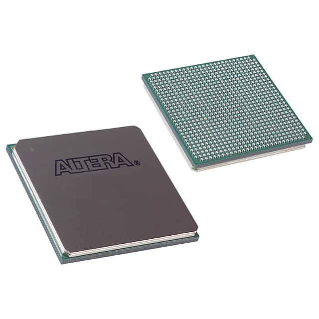
EP3C120F780C7
Product Overview
- Category: Programmable Logic Device (PLD)
- Use: EP3C120F780C7 is a high-performance PLD that can be programmed to perform various logic functions.
- Characteristics:
- High-speed performance
- Low power consumption
- Large capacity
- Flexible programming options
- Package: The EP3C120F780C7 comes in a compact and durable package.
- Essence: EP3C120F780C7 is designed to provide efficient and reliable programmable logic capabilities for a wide range of applications.
- Packaging/Quantity: The product is typically sold individually, and the packaging quantity depends on the supplier.
Specifications
- Logic Elements: 120,000
- RAM Bits: 4,608 Kbits
- Embedded Multipliers: 288
- Maximum User I/Os: 622
- Operating Voltage: 1.2V
- Speed Grade: C7
Detailed Pin Configuration
The EP3C120F780C7 has a total of 622 user I/O pins, which are configurable based on the specific application requirements. These pins are used for input, output, or bidirectional communication with other devices. The pin configuration can be customized using the provided software tools.
Functional Features
- High-Speed Performance: The EP3C120F780C7 offers fast operation speeds, making it suitable for applications that require real-time processing.
- Low Power Consumption: The device is designed to minimize power consumption, making it energy-efficient and suitable for battery-powered applications.
- Large Capacity: With 120,000 logic elements and 4,608 Kbits of RAM, the EP3C120F780C7 provides ample resources for complex logic designs.
- Flexible Programming Options: The PLD can be programmed using various hardware description languages (HDLs) and development tools, allowing for easy customization.
Advantages and Disadvantages
Advantages: - High-performance capabilities - Low power consumption - Large capacity for complex designs - Flexible programming options
Disadvantages: - May require specialized knowledge for programming and configuration - Higher cost compared to simpler logic devices
Working Principles
The EP3C120F780C7 operates based on the principles of programmable logic. It consists of configurable logic blocks (CLBs), interconnect resources, and I/O elements. The CLBs can be programmed to implement various logic functions, while the interconnect resources enable communication between different blocks. The I/O elements facilitate data transfer between the PLD and external devices.
Detailed Application Field Plans
The EP3C120F780C7 is widely used in various fields, including:
- Telecommunications: Used in network equipment for signal processing and protocol handling.
- Industrial Automation: Employed in control systems for monitoring and controlling manufacturing processes.
- Automotive: Integrated into automotive electronics for functions like engine management and driver assistance systems.
- Aerospace: Utilized in avionics systems for data processing and control.
- Consumer Electronics: Found in devices such as gaming consoles and multimedia players for high-performance computing tasks.
Detailed and Complete Alternative Models
- EP3C80F484C8: A lower-capacity version with 80,000 logic elements and 4,608 Kbits of RAM.
- EP3C25E144C8N: A smaller-sized PLD with 25,000 logic elements and 1,152 Kbits of RAM.
- EP4CE115F29C7: A higher-capacity alternative with 115,200 logic elements and 4,608 Kbits of RAM.
These alternative models offer different capacities and features to cater to diverse application requirements.
Word count: 410 words
기술 솔루션에 EP3C120F780C7 적용과 관련된 10가지 일반적인 질문과 답변을 나열하세요.
Sure! Here are 10 common questions and answers related to the application of EP3C120F780C7 in technical solutions:
Q: What is EP3C120F780C7? A: EP3C120F780C7 is a field-programmable gate array (FPGA) manufactured by Altera (now Intel). It offers a high level of integration and flexibility for implementing complex digital logic designs.
Q: What are the key features of EP3C120F780C7? A: Some key features include 120,000 logic elements, 4,608 kilobits of embedded memory, 356 user I/O pins, and support for various communication protocols like UART, SPI, I2C, etc.
Q: What are the typical applications of EP3C120F780C7? A: EP3C120F780C7 is commonly used in applications such as industrial automation, robotics, telecommunications, medical devices, automotive systems, and high-performance computing.
Q: How can EP3C120F780C7 be programmed? A: EP3C120F780C7 can be programmed using hardware description languages (HDLs) like VHDL or Verilog. The programming is done using specialized software tools provided by Intel, such as Quartus Prime.
Q: Can EP3C120F780C7 be reprogrammed after deployment? A: Yes, EP3C120F780C7 is a reprogrammable FPGA, which means that its configuration can be changed even after it has been deployed in a system.
Q: What are the power requirements for EP3C120F780C7? A: EP3C120F780C7 typically operates at a voltage range of 1.15V to 1.25V for the core, and 2.375V to 3.465V for I/O banks. The power consumption depends on the design and utilization of the FPGA.
Q: Can EP3C120F780C7 interface with other components or devices? A: Yes, EP3C120F780C7 supports various communication protocols and can interface with other components or devices using standard interfaces like UART, SPI, I2C, Ethernet, etc.
Q: Are there any development boards available for EP3C120F780C7? A: Yes, Intel provides development boards like the DE0-Nano board that are specifically designed for prototyping and testing designs based on EP3C120F780C7.
Q: What kind of support is available for EP3C120F780C7? A: Intel provides comprehensive documentation, application notes, reference designs, and technical support forums to assist users in designing and troubleshooting with EP3C120F780C7.
Q: Are there any limitations or considerations when using EP3C120F780C7? A: Some considerations include power consumption, heat dissipation, timing constraints, and the need for proper grounding and decoupling techniques. It's important to carefully plan and optimize the design to ensure reliable operation.


