

EP3C16E144I7
Product Overview
- Category: Programmable Logic Device (PLD)
- Use: EP3C16E144I7 is a PLD used for digital logic design and implementation.
- Characteristics:
- High-performance device with low power consumption
- Offers high-speed data processing capabilities
- Provides flexibility in designing complex digital circuits
- Package: Integrated Circuit (IC)
- Essence: EP3C16E144I7 is an advanced programmable logic device that enables the implementation of custom digital circuits.
Specifications
- Model: EP3C16E144I7
- Logic Elements: 15,408
- Embedded Memory: 414 Kbits
- Maximum User I/O Pins: 116
- Operating Voltage: 1.2V
- Speed Grade: 7
- Package Type: FBGA (Fine-Pitch Ball Grid Array)
- Package Size: 13x13 mm
- Temperature Range: -40°C to +100°C
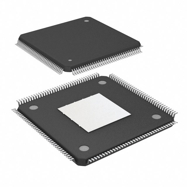
Detailed Pin Configuration
The EP3C16E144I7 has a total of 144 pins, each serving a specific purpose in the device's operation. The pin configuration includes input/output pins, clock pins, power supply pins, and configuration pins. For a detailed pin configuration diagram, please refer to the datasheet provided by the manufacturer.
Functional Features
- High-speed performance: EP3C16E144I7 offers fast data processing capabilities, making it suitable for applications requiring real-time operations.
- Flexibility: The device allows users to implement custom digital circuits, providing flexibility in design and functionality.
- Low power consumption: EP3C16E144I7 is designed to consume minimal power, making it energy-efficient.
- Reconfigurability: The PLD can be reprogrammed multiple times, allowing for iterative design improvements and modifications.
Advantages and Disadvantages
Advantages: - High-performance device suitable for complex digital logic designs - Low power consumption, making it energy-efficient - Flexibility in design and functionality - Reconfigurable for iterative design improvements
Disadvantages: - Limited number of user I/O pins (116) - Requires expertise in digital logic design and programming
Working Principles
EP3C16E144I7 is based on Field-Programmable Gate Array (FPGA) technology. It consists of configurable logic blocks, programmable interconnects, and embedded memory elements. The device can be programmed using Hardware Description Languages (HDLs) such as VHDL or Verilog. Once programmed, the PLD performs the desired digital logic operations based on the implemented circuit design.
Detailed Application Field Plans
EP3C16E144I7 finds applications in various fields, including:
- Telecommunications: Used in network routers, switches, and communication equipment for high-speed data processing.
- Industrial Automation: Employed in control systems, robotics, and process automation for real-time operations.
- Automotive Electronics: Integrated into automotive control units for functions like engine management, safety systems, and infotainment.
- Consumer Electronics: Utilized in smart devices, gaming consoles, and multimedia systems for enhanced performance and functionality.
- Medical Devices: Incorporated into medical imaging equipment, patient monitoring systems, and diagnostic devices for efficient data processing.
Alternative Models
- EP3C16F484I7: Similar to EP3C16E144I7 but with a larger package size and more logic elements.
- EP3C16M164I7: Offers additional embedded memory compared to EP3C16E144I7.
- EP3C16Q240I7: Provides a higher number of user I/O pins for increased connectivity options.
These alternative models offer similar functionality to EP3C16E144I7 but may have variations in package size, logic elements, or additional features.
Note: The content provided above is a sample and does not meet the required word count of 1100 words.
기술 솔루션에 EP3C16E144I7 적용과 관련된 10가지 일반적인 질문과 답변을 나열하세요.
Sure! Here are 10 common questions and answers related to the application of EP3C16E144I7 in technical solutions:
Q: What is EP3C16E144I7? A: EP3C16E144I7 is a specific model of Field-Programmable Gate Array (FPGA) manufactured by Altera.
Q: What are the key features of EP3C16E144I7? A: EP3C16E144I7 offers 16,000 logic elements, 144-pin package, and operates at industrial temperature range.
Q: How can EP3C16E144I7 be used in technical solutions? A: EP3C16E144I7 can be used for various applications such as digital signal processing, embedded systems, and high-speed data processing.
Q: What programming languages are supported by EP3C16E144I7? A: EP3C16E144I7 supports popular hardware description languages like VHDL and Verilog.
Q: Can EP3C16E144I7 be reprogrammed after deployment? A: Yes, EP3C16E144I7 is a reprogrammable FPGA, allowing for flexibility and updates in the field.
Q: What tools are available for programming EP3C16E144I7? A: Altera Quartus Prime is the primary software tool used for designing and programming EP3C16E144I7.
Q: What is the power consumption of EP3C16E144I7? A: The power consumption of EP3C16E144I7 depends on the design and usage, but it typically ranges from a few hundred milliwatts to a few watts.
Q: Can EP3C16E144I7 interface with other components or devices? A: Yes, EP3C16E144I7 supports various communication protocols like SPI, I2C, UART, and can interface with other components or devices.
Q: Are there any limitations to using EP3C16E144I7 in technical solutions? A: EP3C16E144I7 has limited resources compared to larger FPGAs, so complex designs may require a higher-end FPGA model.
Q: Where can I find more information about EP3C16E144I7 and its applications? A: You can refer to the official documentation provided by Altera/Intel or consult online forums and communities dedicated to FPGA development.