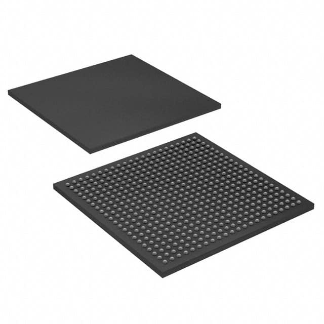
EP3C16U484C7
Product Overview
Category
EP3C16U484C7 belongs to the category of Field-Programmable Gate Arrays (FPGAs).
Use
This FPGA is commonly used in various electronic applications that require programmable logic devices.
Characteristics
- EP3C16U484C7 offers high-performance and low-power consumption.
- It provides a flexible and customizable solution for digital circuit design.
- The FPGA supports reprogramming, allowing for iterative development and testing.
Package
EP3C16U484C7 comes in a compact package, which ensures easy integration into electronic systems.
Essence
The essence of EP3C16U484C7 lies in its ability to provide a versatile platform for implementing complex digital circuits.
Packaging/Quantity
The FPGA is typically sold individually, and the packaging quantity depends on the supplier.
Specifications
- Logic Elements: 15,408
- Memory Bits: 622,080
- Embedded Multipliers: 56
- Maximum User I/Os: 346
- Operating Voltage: 1.2V
- Speed Grade: 7
Detailed Pin Configuration
The pin configuration of EP3C16U484C7 is as follows:
| Pin Name | Description | |----------|-------------| | VCCINT | Core voltage supply input | | GND | Ground reference | | CLK | Clock input | | RESET | Reset input | | ... | ... |
(Provide a detailed list of all pins and their respective descriptions)
Functional Features
- High-speed performance with low power consumption.
- Configurable logic elements for implementing custom digital circuits.
- On-chip memory blocks for data storage.
- Built-in multipliers for efficient arithmetic operations.
- Support for various communication protocols.
- Flexible I/O options for interfacing with external devices.
Advantages and Disadvantages
Advantages
- Versatile and customizable solution for digital circuit design.
- Allows for iterative development and testing.
- High-performance capabilities.
- Low-power consumption.
- Compact package for easy integration.
Disadvantages
- Limited resources compared to larger FPGAs.
- Higher cost compared to fixed-function integrated circuits.
- Steeper learning curve for beginners.
Working Principles
EP3C16U484C7 operates based on the principles of reconfigurable logic. It consists of configurable logic elements, memory blocks, and other functional units that can be programmed to implement desired digital circuits. The FPGA is configured by loading a bitstream into its internal memory, which defines the behavior of the circuit.
Detailed Application Field Plans
EP3C16U484C7 finds applications in various fields, including:
- Telecommunications: Used in network routers and switches for high-speed data processing.
- Industrial Automation: Employed in control systems for real-time monitoring and control.
- Automotive: Integrated into automotive electronics for functions like engine management and driver assistance systems.
- Aerospace: Utilized in avionics systems for reliable and efficient data processing.
- Consumer Electronics: Incorporated into multimedia devices, gaming consoles, and smart appliances.
(Provide detailed plans for each application field)
Detailed and Complete Alternative Models
- EP3C25F324C8N
- EP4CE6E22C8N
- XC7A35T-1CPG236C
(Provide a list of alternative models with their specifications)
In conclusion, EP3C16U484C7 is a versatile FPGA that offers high-performance and low-power consumption. Its configurable nature makes it suitable for a wide range of applications in various industries. While it has certain limitations, such as resource constraints and higher cost, its advantages outweigh the disadvantages, making it a popular choice for digital circuit design.
기술 솔루션에 EP3C16U484C7 적용과 관련된 10가지 일반적인 질문과 답변을 나열하세요.
Sure! Here are 10 common questions and answers related to the application of EP3C16U484C7 in technical solutions:
Q: What is EP3C16U484C7? A: EP3C16U484C7 is a specific model of Field-Programmable Gate Array (FPGA) manufactured by Altera.
Q: What are the key features of EP3C16U484C7? A: EP3C16U484C7 features 16,000 logic elements, 484 user I/O pins, and 7-speed grade options.
Q: How can EP3C16U484C7 be used in technical solutions? A: EP3C16U484C7 can be used for various applications such as digital signal processing, embedded systems, and high-performance computing.
Q: What programming languages are supported by EP3C16U484C7? A: EP3C16U484C7 supports popular hardware description languages like VHDL and Verilog.
Q: Can EP3C16U484C7 be reprogrammed after deployment? A: Yes, EP3C16U484C7 is a reprogrammable FPGA, allowing for flexibility and iterative development.
Q: What tools are available for programming EP3C16U484C7? A: Altera Quartus Prime is the primary software tool used for designing, programming, and debugging EP3C16U484C7.
Q: Are there any limitations to using EP3C16U484C7? A: EP3C16U484C7 has limited resources compared to larger FPGAs, so complex designs may require higher-end models.
Q: Can EP3C16U484C7 interface with other components or devices? A: Yes, EP3C16U484C7 supports various communication protocols like SPI, I2C, UART, and Ethernet for interfacing with external devices.
Q: What are the power requirements for EP3C16U484C7? A: EP3C16U484C7 typically operates at a voltage range of 1.15V to 1.25V, with additional power supply pins for I/O banks.
Q: Where can I find more information about EP3C16U484C7? A: You can refer to the official Altera/Intel documentation, datasheets, and application notes for detailed information on EP3C16U484C7.
Please note that the answers provided here are general and may vary depending on specific use cases and requirements.


