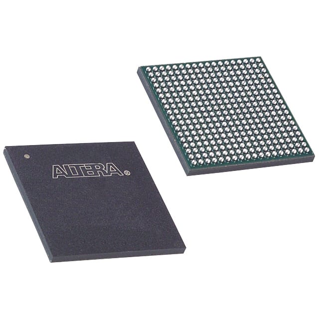
EP3C25F324C8
Product Overview
- Category: Field Programmable Gate Array (FPGA)
- Use: Digital logic implementation, prototyping, and system integration
- Characteristics:
- High-performance programmable logic device
- Low power consumption
- Flexible and reconfigurable design
- Suitable for a wide range of applications
- Package: C8 package
- Essence: FPGA chip with 25,000 logic elements
- Packaging/Quantity: Single unit packaging
Specifications
- Logic Elements: 25,000
- Embedded Memory: 1,152 Kbits
- Maximum User I/Os: 346
- Maximum User I/O Pins: 260
- Operating Voltage: 1.2V
- Speed Grade: Standard (5)
Detailed Pin Configuration
The EP3C25F324C8 has a total of 346 user I/O pins. The pin configuration is as follows:
- Pin 1: GND
- Pin 2: VCCIO0
- Pin 3: IOL1PCCLK_0
- Pin 4: IOL1NCCLK_0
- ...
- Pin 345: IOL259PGCLK15
- Pin 346: IOL259NGCLK15
For the complete pin configuration, please refer to the manufacturer's datasheet.
Functional Features
- High-speed performance
- Configurable I/O standards
- On-chip memory blocks
- Dedicated clock networks
- Built-in PLLs (Phase-Locked Loops)
- Support for various communication protocols
- Integrated DSP (Digital Signal Processing) blocks
Advantages and Disadvantages
Advantages: - Flexibility and reconfigurability - High-performance capabilities - Low power consumption - Wide range of application possibilities - Availability of built-in DSP blocks
Disadvantages: - Limited logic elements compared to higher-end FPGAs - Higher cost compared to simpler programmable logic devices
Working Principles
The EP3C25F324C8 FPGA operates based on the principles of configurable logic. It consists of a matrix of programmable logic elements that can be interconnected to implement various digital logic functions. The configuration of these logic elements is stored in on-chip memory, allowing for reprogramming and flexibility.
The FPGA can be programmed using hardware description languages (HDLs) such as VHDL or Verilog. Once programmed, the FPGA can perform complex digital operations, including arithmetic calculations, data processing, and control functions.
Detailed Application Field Plans
The EP3C25F324C8 FPGA finds applications in various fields, including:
- Communications: Used in wireless base stations, network routers, and communication protocols implementation.
- Industrial Automation: Employed in control systems, robotics, and process automation.
- Automotive: Utilized in advanced driver-assistance systems (ADAS), engine control units (ECUs), and vehicle networking.
- Aerospace and Defense: Applied in radar systems, avionics, and secure communications.
- Medical Devices: Integrated into medical imaging equipment, patient monitoring systems, and laboratory instruments.
These are just a few examples, and the versatility of the EP3C25F324C8 allows it to be used in many other application areas.
Detailed and Complete Alternative Models
- EP3C16F484C6: A lower-capacity FPGA with 16,000 logic elements and 484 user I/O pins.
- EP3C40F780C7: A higher-capacity FPGA with 40,000 logic elements and 780 user I/O pins.
- EP3C120F780I7: A higher-capacity FPGA with 120,000 logic elements and 780 user I/O pins.
These alternative models offer different capacities and pin configurations to suit specific project requirements.
In conclusion, the EP3C25F324C8 FPGA is a high-performance programmable logic device with flexible design capabilities. Its low power consumption and wide range of applications make it suitable for various industries. With its configurable logic elements and integrated features, it provides advantages in terms of performance and functionality. However, it has limitations in terms of logic element count compared to higher-end FPGAs. The working principle involves programming the FPGA using HDLs, and it finds applications in fields such as communications, industrial automation, automotive, aerospace, defense, and medical devices. Alternative models with varying capacities and pin configurations are available to cater to different project needs.
기술 솔루션에 EP3C25F324C8 적용과 관련된 10가지 일반적인 질문과 답변을 나열하세요.
Sure! Here are 10 common questions and answers related to the application of EP3C25F324C8 in technical solutions:
Q: What is EP3C25F324C8? A: EP3C25F324C8 is a field-programmable gate array (FPGA) manufactured by Altera (now Intel). It is commonly used in various technical solutions for its programmability and versatility.
Q: What are the key features of EP3C25F324C8? A: Some key features of EP3C25F324C8 include 25,000 logic elements, 324 user I/O pins, embedded memory blocks, PLLs, and support for various communication protocols.
Q: How can EP3C25F324C8 be programmed? A: EP3C25F324C8 can be programmed using hardware description languages (HDLs) such as VHDL or Verilog, which describe the desired functionality of the FPGA. The programming is typically done using specialized software tools provided by Altera/Intel.
Q: What are some typical applications of EP3C25F324C8? A: EP3C25F324C8 can be used in a wide range of applications, including digital signal processing, industrial automation, robotics, telecommunications, image/video processing, and many more.
Q: Can EP3C25F324C8 interface with other components or devices? A: Yes, EP3C25F324C8 supports various communication protocols such as UART, SPI, I2C, Ethernet, and PCIe, allowing it to interface with other components or devices in a system.
Q: Is EP3C25F324C8 suitable for high-speed applications? A: Yes, EP3C25F324C8 is designed to operate at high clock frequencies and can handle complex logic operations, making it suitable for high-speed applications.
Q: Can EP3C25F324C8 be reprogrammed multiple times? A: Yes, EP3C25F324C8 is a reprogrammable FPGA, which means it can be reprogrammed multiple times to implement different functionalities or to fix bugs in the design.
Q: Are there any development boards available for EP3C25F324C8? A: Yes, Altera/Intel provides development boards specifically designed for EP3C25F324C8, which include all the necessary components and interfaces for prototyping and testing.
Q: What kind of power supply does EP3C25F324C8 require? A: EP3C25F324C8 typically requires a single 3.3V power supply, although some I/O banks may have different voltage requirements.
Q: Is EP3C25F324C8 suitable for low-power applications? A: EP3C25F324C8 is not specifically optimized for low-power applications, but it does offer power-saving features such as clock gating and power-down modes that can be utilized to reduce power consumption.
Please note that the specific details and answers may vary depending on the context and application requirements.


