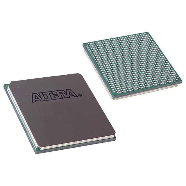
EP4CE115F29I7
Product Overview
- Category: Integrated Circuit (IC)
- Use: Programmable Logic Device (PLD)
- Characteristics: High-performance, low-power consumption
- Package: 1152-pin FineLine BGA
- Essence: Field-Programmable Gate Array (FPGA)
- Packaging/Quantity: Tray, 1 unit
Specifications
- Manufacturer: Intel Corporation
- Family: Cyclone IV E
- Device: EP4CE115F29I7
- Technology: 40nm
- Logic Elements: 114,480
- Embedded Multipliers: 288
- Memory Blocks: 4,608
- Maximum User I/Os: 622
- Operating Voltage: 1.2V
- Speed Grade: 7
Detailed Pin Configuration
The EP4CE115F29I7 has a total of 1152 pins, which are organized into various groups for different functionalities. The pin configuration includes power supply pins, ground pins, configuration pins, clock pins, input/output pins, and dedicated pins for specific functions such as memory interfaces, high-speed serial communication, and external memory interfaces.
For the detailed pin configuration diagram, please refer to the datasheet provided by the manufacturer.
Functional Features
- High-performance FPGA with advanced architecture
- Low-power consumption design for energy-efficient applications
- Flexible and reprogrammable logic elements for customization
- Embedded multipliers for efficient digital signal processing
- Large memory blocks for data storage and retrieval
- Support for various communication protocols and interfaces
- Robust design with built-in error detection and correction mechanisms
Advantages and Disadvantages
Advantages: - Versatile and adaptable for a wide range of applications - High-performance capabilities for complex tasks - Lower power consumption compared to alternative solutions - Cost-effective due to reprogrammability - Extensive support and resources available from the manufacturer
Disadvantages: - Limited I/O count compared to higher-end FPGA models - Relatively large package size may require more board space - Steeper learning curve for beginners due to complexity
Working Principles
The EP4CE115F29I7 is based on the field-programmable gate array (FPGA) technology. It consists of a matrix of programmable logic elements interconnected through configurable routing channels. The device can be programmed to implement various digital circuits by configuring the interconnections and functionality of these logic elements.
The working principle involves loading a configuration bitstream into the FPGA, which defines the desired circuit functionality. Once programmed, the FPGA operates as a dedicated digital circuit, executing the desired operations based on the input signals and internal logic configuration.
Detailed Application Field Plans
The EP4CE115F29I7 finds applications in various fields, including but not limited to:
- Telecommunications: Used in base stations, network routers, and communication infrastructure equipment.
- Industrial Automation: Employed in control systems, robotics, and factory automation.
- Automotive: Integrated into automotive electronics for advanced driver assistance systems (ADAS), infotainment, and engine control units (ECUs).
- Aerospace and Defense: Utilized in avionics, radar systems, and military-grade communication equipment.
- Medical Devices: Incorporated into medical imaging systems, patient monitoring devices, and laboratory equipment.
Detailed and Complete Alternative Models
- EP4CE30F23C8N: A lower-cost alternative with fewer logic elements and I/Os.
- EP4CE55F23I7N: A mid-range option with intermediate logic capacity and I/O count.
- EP4CE115F29C7N: A variant with the same logic capacity but different package and pin configuration.
- EP4CE150F29I7N: A higher-end model with increased logic capacity and I/O count.
These alternative models provide different trade-offs in terms of cost, performance, and pin compatibility, allowing users to choose the most suitable option for their specific requirements.
Note: The above information is based on the available data at the time of writing. For the most accurate and up-to-date specifications, please refer to the manufacturer's datasheet.
기술 솔루션에 EP4CE115F29I7 적용과 관련된 10가지 일반적인 질문과 답변을 나열하세요.
Sure! Here are 10 common questions and answers related to the application of EP4CE115F29I7 in technical solutions:
Q: What is EP4CE115F29I7? A: EP4CE115F29I7 is a field-programmable gate array (FPGA) chip manufactured by Intel (formerly Altera). It offers a high level of performance and flexibility for various technical applications.
Q: What are the key features of EP4CE115F29I7? A: Some key features of EP4CE115F29I7 include 115,200 logic elements, 3,888 embedded memory blocks, 266 user I/O pins, and support for various communication protocols.
Q: What are the typical applications of EP4CE115F29I7? A: EP4CE115F29I7 is commonly used in applications such as digital signal processing, image and video processing, industrial automation, robotics, telecommunications, and high-performance computing.
Q: How can EP4CE115F29I7 be programmed? A: EP4CE115F29I7 can be programmed using hardware description languages (HDLs) like VHDL or Verilog, which describe the desired functionality of the FPGA. The programming is typically done using specialized software tools provided by Intel.
Q: Can EP4CE115F29I7 be reprogrammed after it has been programmed once? A: Yes, EP4CE115F29I7 is a reprogrammable FPGA, meaning that its configuration can be changed multiple times, allowing for flexibility in design iterations and updates.
Q: What kind of power supply does EP4CE115F29I7 require? A: EP4CE115F29I7 requires a single 3.3V power supply for its core voltage, and additional voltages may be required for I/O banks depending on the specific application.
Q: Can EP4CE115F29I7 interface with other components or devices? A: Yes, EP4CE115F29I7 supports various communication protocols such as UART, SPI, I2C, Ethernet, and PCIe, allowing it to interface with other components or devices in a system.
Q: What kind of development boards are available for EP4CE115F29I7? A: Intel provides development boards like the DE2-115 board, which is specifically designed for EP4CE115F29I7. These boards offer a platform for prototyping and testing FPGA designs.
Q: Are there any limitations or considerations when using EP4CE115F29I7? A: Some considerations include power consumption, heat dissipation, and the need for proper grounding and decoupling techniques. Additionally, complex designs may require careful optimization to fit within the available resources of the FPGA.
Q: Where can I find technical support or documentation for EP4CE115F29I7? A: You can find technical support, datasheets, reference designs, and user guides for EP4CE115F29I7 on Intel's website or by contacting their customer support. Additionally, online forums and communities dedicated to FPGA development can provide valuable insights and assistance.


