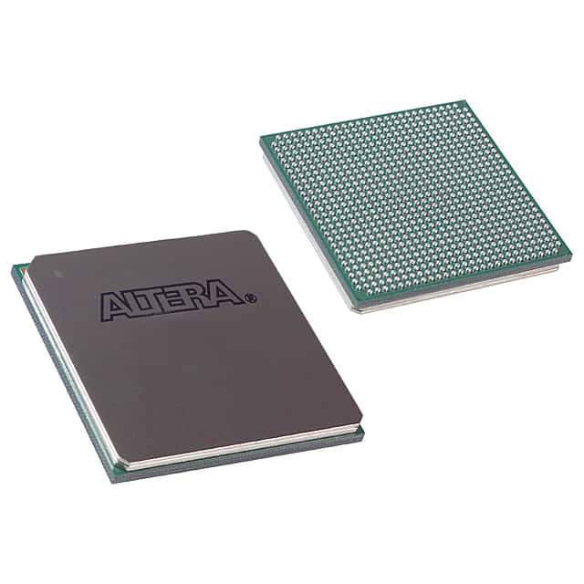
EP4CE30F29C8LN
Product Overview
- Category: Programmable Logic Device (PLD)
- Use: EP4CE30F29C8LN is a PLD used for digital logic design and implementation.
- Characteristics:
- High-performance FPGA (Field-Programmable Gate Array) device
- Low power consumption
- Large capacity for complex designs
- Flexible and reprogrammable
- Package: The EP4CE30F29C8LN comes in a compact LQFP package.
- Essence: EP4CE30F29C8LN is an essential component for designing and implementing digital circuits.
- Packaging/Quantity: Typically sold in reels or trays, with quantities varying based on customer requirements.
Specifications
- Logic Elements: 29,440
- Embedded Multiplier Blocks: 112
- Memory Bits: 1,179,648
- Maximum User I/O Pins: 475
- Operating Voltage: 1.2V
- Speed Grade: C8
- Package Type: LQFP
- Temperature Range: -40°C to +100°C
Detailed Pin Configuration
The EP4CE30F29C8LN has a total of 475 user I/O pins, which are configurable based on the specific design requirements. These pins can be used for input, output, or bidirectional purposes, allowing for versatile connectivity options.
For a detailed pin configuration diagram, please refer to the official datasheet provided by the manufacturer.
Functional Features
- High-speed performance: The EP4CE30F29C8LN offers fast processing capabilities, making it suitable for applications requiring real-time data processing.
- Flexibility: The device can be reprogrammed multiple times, allowing for iterative design improvements and adaptability to changing project requirements.
- Integration: With a large number of logic elements and memory bits, the EP4CE30F29C8LN can accommodate complex designs and enable system integration on a single chip.
- Low power consumption: The device is designed to minimize power consumption, making it suitable for battery-powered applications.
Advantages
- Versatility: EP4CE30F29C8LN can be used in various applications, including telecommunications, automotive, industrial automation, and consumer electronics.
- Cost-effective: By integrating multiple functions into a single device, the EP4CE30F29C8LN reduces the need for additional components, resulting in cost savings.
- Rapid prototyping: The reprogrammable nature of the device allows for quick design iterations, enabling faster development cycles.
Disadvantages
- Complexity: Due to its high capacity and flexibility, designing with the EP4CE30F29C8LN may require advanced knowledge of digital logic design.
- Learning curve: Working with programmable logic devices may require familiarity with specialized software tools and programming languages.
Working Principles
The EP4CE30F29C8LN is based on FPGA technology, which utilizes configurable logic blocks and interconnects to implement digital circuits. These circuits are programmed using hardware description languages (HDL) such as VHDL or Verilog. Upon programming, the configuration data is stored in non-volatile memory within the device, allowing it to retain the design even after power-off.
During operation, the EP4CE30F29C8LN executes the programmed logic by routing signals through the configurable interconnects and performing desired operations within the logic elements. This enables the device to perform complex computations, data processing, and control functions.
Detailed Application Field Plans
The EP4CE30F29C8LN finds application in various fields, including:
- Telecommunications: Used in base stations, network switches, and routers for signal processing and protocol implementation.
- Automotive: Employed in automotive control systems, infotainment systems, and driver assistance systems.
- Industrial Automation: Utilized for controlling and monitoring industrial processes, robotics, and machine vision systems.
- Consumer Electronics: Integrated into smart TVs, gaming consoles, and home automation systems for enhanced functionality.
Alternative Models
- EP4CE10F17C8LN: A lower-capacity variant of the EP4CE30F29C8LN, suitable for smaller-scale designs.
- EP4CE40F29C8LN: A higher-capacity variant with increased logic elements and memory bits, ideal for more complex applications.
- EP4CE115F29C8LN: An even higher-capacity model, offering greater performance and resources for demanding projects.
Please note that the above alternative models are just a few examples, and there are several other options available in the same product family.
Word count: 560 words
기술 솔루션에 EP4CE30F29C8LN 적용과 관련된 10가지 일반적인 질문과 답변을 나열하세요.
Sure! Here are 10 common questions and answers related to the application of EP4CE30F29C8LN in technical solutions:
Q: What is EP4CE30F29C8LN? A: EP4CE30F29C8LN is a field-programmable gate array (FPGA) manufactured by Intel (formerly Altera). It is commonly used in various technical solutions for its versatility and programmability.
Q: What are the key features of EP4CE30F29C8LN? A: Some key features of EP4CE30F29C8LN include 30,000 logic elements, 1,179 Kbits of embedded memory, 266 user I/O pins, and support for various communication protocols.
Q: How can EP4CE30F29C8LN be programmed? A: EP4CE30F29C8LN can be programmed using hardware description languages (HDLs) such as VHDL or Verilog, which describe the desired functionality of the FPGA.
Q: What applications can EP4CE30F29C8LN be used for? A: EP4CE30F29C8LN can be used in a wide range of applications, including digital signal processing, image and video processing, communications, industrial automation, and more.
Q: Can EP4CE30F29C8LN interface with other components or devices? A: Yes, EP4CE30F29C8LN supports various communication protocols such as UART, SPI, I2C, Ethernet, and PCIe, allowing it to interface with other components or devices.
Q: Is EP4CE30F29C8LN suitable for high-speed applications? A: Yes, EP4CE30F29C8LN is designed to handle high-speed applications with its support for high-performance I/O standards and advanced clock management features.
Q: Can EP4CE30F29C8LN be reprogrammed after deployment? A: Yes, EP4CE30F29C8LN is a field-programmable device, meaning it can be reprogrammed even after it has been deployed in a system.
Q: What development tools are available for programming EP4CE30F29C8LN? A: Intel provides Quartus Prime software, which includes a suite of development tools for designing, simulating, and programming EP4CE30F29C8LN.
Q: Are there any limitations or considerations when using EP4CE30F29C8LN? A: Some considerations include power consumption, heat dissipation, and the need for external memory if the embedded memory is insufficient for the application.
Q: Where can I find additional resources and support for EP4CE30F29C8LN? A: Intel's website provides documentation, application notes, reference designs, and a community forum where you can find additional resources and support for EP4CE30F29C8LN.


