

EP4CGX15BF14C7
Product Overview
- Category: Programmable Logic Device (PLD)
- Use: EP4CGX15BF14C7 is a PLD used for digital logic design and implementation.
- Characteristics: It offers high-performance, low-power consumption, and flexibility in designing complex digital systems.
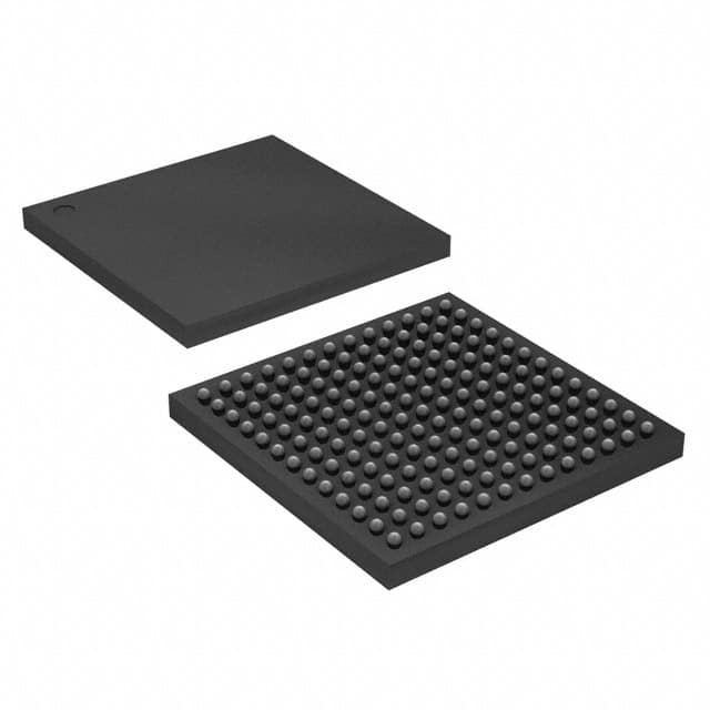
- Package: The EP4CGX15BF14C7 comes in a compact BGA package.
- Essence: This PLD provides a reconfigurable hardware platform for implementing various digital circuits.
- Packaging/Quantity: The EP4CGX15BF14C7 is typically sold individually.
Specifications
- Logic Elements: 15,408
- Embedded Memory: 414 Kbits
- Maximum User I/Os: 622
- Operating Voltage: 1.2V
- Operating Temperature: -40°C to +100°C
- Speed Grade: 7
Detailed Pin Configuration
The EP4CGX15BF14C7 has a total of 622 pins, which are divided into different categories:
- I/O Pins: These pins are used for input/output operations and connect the device to external components.
- Power Pins: These pins provide power supply to the device.
- Configuration Pins: These pins are used for configuring the PLD during startup.
- Clock Pins: These pins receive clock signals for synchronous operation.
- JTAG Pins: These pins are used for programming and debugging the device.
For a detailed pin configuration diagram, please refer to the datasheet provided by the manufacturer.
Functional Features
- High Performance: The EP4CGX15BF14C7 offers fast processing speeds and efficient utilization of resources.
- Low Power Consumption: It is designed to minimize power consumption, making it suitable for battery-powered applications.
- Flexibility: The PLD allows for reconfiguration, enabling designers to modify the functionality of the device as needed.
- Versatility: It supports a wide range of digital logic functions and can be used in various applications.
Advantages and Disadvantages
Advantages: - High-performance processing capabilities - Low power consumption - Flexibility in design and implementation - Versatile application possibilities
Disadvantages: - Limited number of I/O pins compared to higher-end models - Higher cost compared to simpler programmable logic devices
Working Principles
The EP4CGX15BF14C7 is based on a Field-Programmable Gate Array (FPGA) architecture. It consists of configurable logic blocks, embedded memory, and input/output circuitry. The device can be programmed using Hardware Description Languages (HDLs) such as VHDL or Verilog. Once programmed, the PLD can perform complex digital logic operations by routing signals through its configurable logic blocks.
Detailed Application Field Plans
The EP4CGX15BF14C7 can be used in various applications, including:
- Embedded Systems: It can be utilized in designing embedded systems for industrial automation, robotics, and IoT devices.
- Digital Signal Processing: The PLD's high-performance capabilities make it suitable for implementing digital signal processing algorithms.
- Communications: It can be used in networking equipment, such as routers and switches, to handle data processing and packet forwarding.
- Video and Image Processing: The device can be employed in video and image processing applications, such as real-time video streaming and image recognition.
Detailed and Complete Alternative Models
- EP4CE6E22C8N
- EP4CE10E22C8N
- EP4CE15E22C8N
- EP4CE30E22C8N
- EP4CE40E22C8N
These alternative models offer similar functionality and performance but may have different specifications and pin configurations. It is recommended to consult the manufacturer's datasheets for detailed information on each model.
Note: The content provided above is a sample entry and may not reflect the actual specifications and details of the EP4CGX15BF14C7 or its alternative models.
기술 솔루션에 EP4CGX15BF14C7 적용과 관련된 10가지 일반적인 질문과 답변을 나열하세요.
Sure! Here are 10 common questions and answers related to the application of EP4CGX15BF14C7 in technical solutions:
Q: What is EP4CGX15BF14C7? A: EP4CGX15BF14C7 is a specific model of field-programmable gate array (FPGA) manufactured by Intel.
Q: What are the key features of EP4CGX15BF14C7? A: Some key features of EP4CGX15BF14C7 include 15,408 logic elements, 504 kilobits of embedded memory, and support for various I/O standards.
Q: What are the typical applications of EP4CGX15BF14C7? A: EP4CGX15BF14C7 is commonly used in applications such as industrial automation, telecommunications, automotive electronics, and medical devices.
Q: How can EP4CGX15BF14C7 be programmed? A: EP4CGX15BF14C7 can be programmed using hardware description languages (HDLs) like VHDL or Verilog, or through graphical programming tools like Quartus Prime.
Q: Can EP4CGX15BF14C7 be reprogrammed after deployment? A: Yes, EP4CGX15BF14C7 is a reprogrammable FPGA, allowing for flexibility and updates even after deployment.
Q: What is the power consumption of EP4CGX15BF14C7? A: The power consumption of EP4CGX15BF14C7 depends on the design and utilization, but it typically ranges from a few hundred milliwatts to a few watts.
Q: Does EP4CGX15BF14C7 support high-speed interfaces? A: Yes, EP4CGX15BF14C7 supports various high-speed interfaces such as PCIe, Ethernet, USB, and DDR3 memory.
Q: Can EP4CGX15BF14C7 interface with other components or microcontrollers? A: Yes, EP4CGX15BF14C7 can interface with other components or microcontrollers using standard protocols like SPI, I2C, UART, or custom communication interfaces.
Q: Are there any development boards available for EP4CGX15BF14C7? A: Yes, Intel provides development boards specifically designed for EP4CGX15BF14C7, which include necessary connectors and peripherals for prototyping and testing.
Q: Where can I find technical documentation and support for EP4CGX15BF14C7? A: You can find technical documentation, datasheets, application notes, and support resources for EP4CGX15BF14C7 on the official Intel website or through their customer support channels.
Please note that the specific details and answers may vary depending on the manufacturer's documentation and product specifications.