

IXTP05N100P
Introduction
The IXTP05N100P is a power MOSFET belonging to the category of semiconductor devices. This device is widely used in various electronic applications due to its unique characteristics and performance.
Basic Information Overview
- Category: Power MOSFET
- Use: Switching and amplification in electronic circuits
- Characteristics: High voltage capability, low on-resistance, fast switching speed
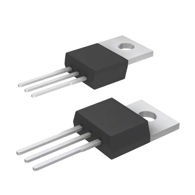
- Package: TO-220AB
- Essence: Efficient power management
- Packaging/Quantity: Typically packaged in reels of 50 or 100 units
Specifications
- Voltage Rating: 1000V
- Current Rating: 5A
- On-Resistance: 1.25Ω
- Gate Threshold Voltage: 2.5V
- Operating Temperature Range: -55°C to 150°C
Detailed Pin Configuration
The IXTP05N100P features a standard TO-220AB package with three pins: 1. Gate (G) 2. Drain (D) 3. Source (S)
Functional Features
- High voltage capability allows for use in high-power applications
- Low on-resistance minimizes power loss and heat generation
- Fast switching speed enables efficient operation in switching circuits
Advantages and Disadvantages
Advantages: - High voltage capability - Low on-resistance - Fast switching speed
Disadvantages: - Higher cost compared to lower voltage MOSFETs - Requires careful handling due to sensitivity to static electricity
Working Principles
The IXTP05N100P operates based on the principle of field-effect transistors, where the flow of current between the drain and source terminals is controlled by the voltage applied to the gate terminal. When a sufficient voltage is applied to the gate, the MOSFET allows current to flow through, enabling it to act as a switch or amplifier in electronic circuits.
Detailed Application Field Plans
The IXTP05N100P finds extensive use in the following application fields: - Power supplies - Motor control - Inverters - Welding equipment - Renewable energy systems
Detailed and Complete Alternative Models
- IXTP01N100P: Lower current rating but similar voltage capability
- IXTP10N100P: Higher current rating and lower on-resistance
- IXTP02N100P: Lower voltage capability but lower cost
In conclusion, the IXTP05N100P power MOSFET offers high voltage capability, low on-resistance, and fast switching speed, making it suitable for a wide range of electronic applications requiring efficient power management and control.
Word Count: 314
기술 솔루션에 IXTP05N100P 적용과 관련된 10가지 일반적인 질문과 답변을 나열하세요.
What is IXTP05N100P?
- IXTP05N100P is a high voltage power MOSFET designed for various technical applications requiring high power handling capabilities.
What is the maximum voltage rating of IXTP05N100P?
- The maximum voltage rating of IXTP05N100P is 1000V.
What is the maximum current rating of IXTP05N100P?
- The maximum continuous drain current rating of IXTP05N100P is 5A.
What are the typical applications of IXTP05N100P?
- Typical applications of IXTP05N100P include power supplies, motor control, inverters, and other high voltage switching applications.
What is the on-state resistance (RDS(on)) of IXTP05N100P?
- The on-state resistance of IXTP05N100P is typically low, providing efficient power handling.
Is IXTP05N100P suitable for high frequency switching applications?
- Yes, IXTP05N100P is designed to handle high frequency switching due to its fast switching characteristics.
Does IXTP05N100P require a heat sink for operation?
- Depending on the application and power dissipation, a heat sink may be required for optimal thermal management.
What is the gate-source voltage (VGS) range for IXTP05N100P?
- The gate-source voltage range for IXTP05N100P is typically ±20V.
Can IXTP05N100P be used in parallel for higher current applications?
- Yes, IXTP05N100P can be used in parallel to increase the overall current handling capability.
Is IXTP05N100P RoHS compliant?
- Yes, IXTP05N100P is RoHS compliant, making it suitable for environmentally conscious designs.