

LC4032B-25TN44C
Product Overview
Category: Integrated Circuit (IC)
Use: The LC4032B-25TN44C is a programmable logic device (PLD) that belongs to the family of Complex Programmable Logic Devices (CPLDs). It is designed for digital circuit applications and offers high flexibility and versatility.
Characteristics: - High-density integration - Low power consumption - Fast performance - Reconfigurable design - Wide operating temperature range
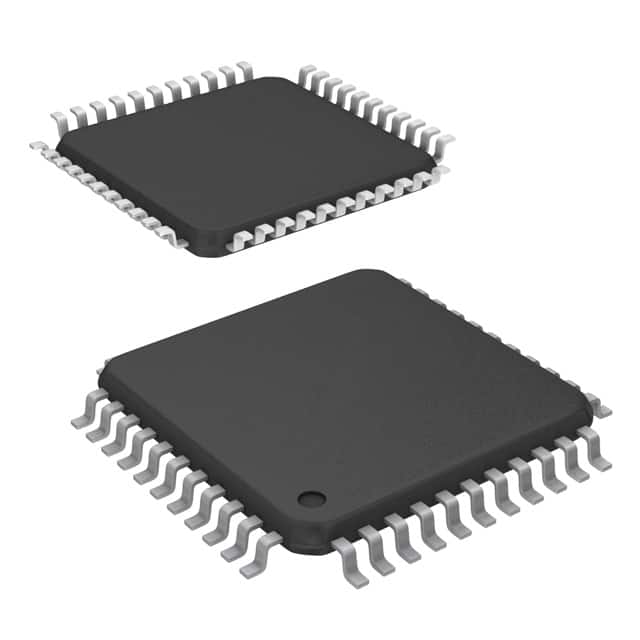
Package: The LC4032B-25TN44C is available in a 44-pin Thin Quad Flat Pack (TQFP) package. This package provides ease of handling and efficient heat dissipation.
Essence: The essence of the LC4032B-25TN44C lies in its ability to implement complex digital circuits with a high degree of customization and reconfiguration.
Packaging/Quantity: The LC4032B-25TN44C is typically sold in reels or trays, with each reel or tray containing a specific quantity of ICs. The exact packaging and quantity may vary depending on the supplier.
Specifications
- Operating Voltage: 3.3V
- Maximum Operating Frequency: 25MHz
- Number of Logic Cells: 32
- Number of I/O Pins: 36
- Programmable Macrocells: 32
- On-Chip Memory: 1,024 bits
- JTAG Boundary Scan Support: Yes
- Package Dimensions: 10mm x 10mm
Detailed Pin Configuration
The LC4032B-25TN44C has a total of 44 pins, each serving a specific purpose. Here is a detailed pin configuration:
- VCCIO - Power supply voltage for I/O pins
- GND - Ground reference
- TCK - Test Clock input for JTAG boundary scan
- TMS - Test Mode Select input for JTAG boundary scan
- TDI - Test Data Input for JTAG boundary scan
- TDO - Test Data Output for JTAG boundary scan
- VCC - Power supply voltage
- GND - Ground reference
- IO0 to IO35 - General-purpose I/O pins
- CLK - Clock input for internal logic
Functional Features
- Programmable Logic: The LC4032B-25TN44C offers a wide range of programmable logic elements, allowing users to implement complex digital circuits.
- Reconfigurability: The device can be reprogrammed multiple times, enabling design changes and updates without the need for hardware modifications.
- Flexible I/O Configuration: The I/O pins can be configured as inputs or outputs, providing versatility in connecting with external devices.
- JTAG Boundary Scan: The built-in JTAG boundary scan support allows for efficient testing and debugging of the device during development and production stages.
Advantages and Disadvantages
Advantages: - High integration density enables compact circuit designs. - Low power consumption makes it suitable for battery-powered applications. - Fast performance ensures efficient execution of digital logic operations. - Reconfigurable nature allows for flexibility in design iterations. - Wide operating temperature range enables usage in various environments.
Disadvantages: - Limited number of logic cells may restrict the complexity of circuits that can be implemented. - Lack of built-in analog components limits its applicability in mixed-signal designs. - Relatively higher cost compared to simpler logic devices.
Working Principles
The LC4032B-25TN44C operates based on the principles of programmable logic. It consists of configurable logic blocks (CLBs), interconnect resources, and I/O elements. The CLBs contain lookup tables (LUTs) that can be programmed to implement desired logic functions. The interconnect resources allow for the routing of signals between different CLBs and I/O pins. The I/O elements provide the interface between the device and external components.
During operation, the LC4032B-25TN44C reads the configuration data from an external memory device and configures its internal logic accordingly. This allows users to define the desired functionality of the device by programming the LUTs and interconnections.
Detailed Application Field Plans
The LC4032B-25TN44C finds applications in various fields where digital circuit implementation is required. Some detailed application field plans include:
- Embedded Systems: The device can be used in embedded systems for controlling and interfacing with peripheral devices.
- Communication Systems: It can be employed in communication systems for protocol handling, signal processing, and data manipulation.
- Industrial Automation: The LC4032B-25TN44C can be utilized in industrial automation systems for control and monitoring purposes.
- Consumer Electronics: It finds applications in consumer electronics products such as gaming consoles, set-top boxes, and home automation systems.
- Automotive Electronics:
기술 솔루션에 LC4032B-25TN44C 적용과 관련된 10가지 일반적인 질문과 답변을 나열하세요.
Sure! Here are 10 common questions and answers related to the application of LC4032B-25TN44C in technical solutions:
1. What is LC4032B-25TN44C? LC4032B-25TN44C is a specific model of Field Programmable Gate Array (FPGA) manufactured by Lattice Semiconductor. It is designed for various applications in digital logic circuits.
2. What are the key features of LC4032B-25TN44C? LC4032B-25TN44C offers 32,768 programmable logic cells, 2,048 Look-Up Tables (LUTs), 32 global clock lines, and 32 I/O pins. It operates at a maximum frequency of 25 MHz and supports various I/O standards.
3. What are some typical applications of LC4032B-25TN44C? LC4032B-25TN44C can be used in a wide range of applications such as industrial automation, telecommunications, automotive electronics, medical devices, consumer electronics, and more.
4. How can LC4032B-25TN44C be programmed? LC4032B-25TN44C can be programmed using Hardware Description Languages (HDLs) like VHDL or Verilog. Design files are compiled into a bitstream that can be loaded onto the FPGA using programming tools provided by Lattice Semiconductor.
5. Can LC4032B-25TN44C be reprogrammed? Yes, LC4032B-25TN44C is a reprogrammable FPGA. The design can be modified and reprogrammed multiple times, allowing for flexibility and iterative development.
6. What are the power requirements for LC4032B-25TN44C? LC4032B-25TN44C typically operates at a voltage range of 3.3V, but it also supports lower voltages like 2.5V or 1.8V. The power consumption depends on the design and utilization of the FPGA.
7. Can LC4032B-25TN44C interface with other components or devices? Yes, LC4032B-25TN44C can interface with various components and devices through its I/O pins. It supports different communication protocols such as SPI, I2C, UART, and more.
8. Are there any development tools available for LC4032B-25TN44C? Lattice Semiconductor provides development tools like Lattice Diamond or Lattice Radiant, which include design software, simulation tools, and programming utilities specifically tailored for their FPGAs.
9. What are the advantages of using LC4032B-25TN44C in technical solutions? LC4032B-25TN44C offers high flexibility, allowing designers to implement complex digital logic circuits. It enables rapid prototyping, reduces time-to-market, and provides cost-effective solutions compared to custom ASIC designs.
10. Where can I find more information about LC4032B-25TN44C? You can find more detailed information about LC4032B-25TN44C, including datasheets, application notes, and reference designs, on the official website of Lattice Semiconductor or by contacting their technical support team.