

LC4064V-10TN44I
Product Overview
Category
The LC4064V-10TN44I belongs to the category of programmable logic devices (PLDs).
Use
This product is commonly used in digital circuit design and implementation. It provides a flexible and customizable solution for various applications.
Characteristics
- Programmable: The LC4064V-10TN44I can be programmed to perform specific functions based on user requirements.
- High Integration: It offers a high level of integration, allowing for complex logic designs in a single device.
- Low Power Consumption: The device is designed to operate efficiently with low power consumption.
- Versatile: It supports a wide range of applications due to its programmability.
Package
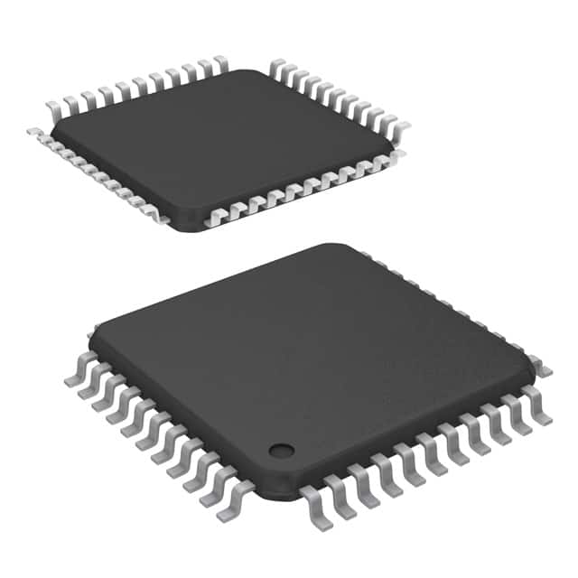
The LC4064V-10TN44I comes in a compact 44-pin Thin Quad Flat Pack (TQFP) package.
Essence
The essence of the LC4064V-10TN44I lies in its ability to provide a reconfigurable logic solution, enabling designers to implement custom digital circuits without the need for dedicated hardware.
Packaging/Quantity
The LC4064V-10TN44I is typically packaged individually and is available in various quantities depending on the manufacturer's specifications.
Specifications
- Device Type: Programmable Logic Device (PLD)
- Model: LC4064V-10TN44I
- Package Type: 44-pin Thin Quad Flat Pack (TQFP)
- Operating Voltage: 3.3V
- Maximum Operating Frequency: 10 MHz
- Number of Logic Cells: 64
- Number of I/O Pins: 36
- Programmable Gates: Yes
- Programmable Flip-Flops: Yes
- Programmable Interconnects: Yes
- Programming Method: In-system programmable (ISP)
Detailed Pin Configuration
The LC4064V-10TN44I has a total of 44 pins, each serving a specific purpose. The pin configuration is as follows:
- VCCIO
- GND
- IO0
- IO1
- IO2
- IO3
- IO4
- IO5
- IO6
- IO7
- IO8
- IO9
- IO10
- IO11
- IO12
- IO13
- IO14
- IO15
- IO16
- IO17
- IO18
- IO19
- IO20
- IO21
- IO22
- IO23
- IO24
- IO25
- IO26
- IO27
- IO28
- IO29
- IO30
- IO31
- IO32
- IO33
- IO34
- IO35
- TCK
- TMS
- TDI
- TDO
- GND
- VCC
Functional Features
The LC4064V-10TN44I offers the following functional features:
- Reconfigurable Logic: The device can be programmed to implement various logic functions.
- Flexible I/O Configuration: It supports a wide range of input and output configurations.
- In-system Programmability: The LC4064V-10TN44I can be programmed while in operation, allowing for dynamic changes to the logic design.
- High-Speed Operation: It operates at a maximum frequency of 10 MHz, enabling efficient processing of digital signals.
Advantages and Disadvantages
Advantages
- Flexibility: The LC4064V-10TN44I provides a flexible solution for digital circuit design, allowing for customization based on specific requirements.
- Cost-Effective: By eliminating the need for dedicated hardware, this PLD reduces overall costs in circuit design and implementation.
- Time-Saving: The programmability of the device enables rapid prototyping and iterative design processes.
Disadvantages
- Limited Complexity: While suitable for many applications, the LC4064V-10TN44I may have limitations in handling highly complex logic designs.
- Learning Curve: Utilizing the full potential of the device requires knowledge of programming languages and digital logic design principles.
Working Principles
The LC4064V-10TN44I operates based on the principles of reconfigurable logic. It consists of programmable gates, flip-flops, and interconnects that can be configured to implement desired logic functions. The device is programmed using specialized software tools that generate a configuration file. This file is then loaded onto the LC4064V-10TN44I, enabling it to perform the desired logic operations.
Detailed Application Field Plans
The LC4064V-10TN44I finds applications in various fields,
기술 솔루션에 LC4064V-10TN44I 적용과 관련된 10가지 일반적인 질문과 답변을 나열하세요.
Sure! Here are 10 common questions and answers related to the application of LC4064V-10TN44I in technical solutions:
Q: What is LC4064V-10TN44I? A: LC4064V-10TN44I is a specific model of a field-programmable gate array (FPGA) manufactured by Lattice Semiconductor.
Q: What are the key features of LC4064V-10TN44I? A: Some key features of LC4064V-10TN44I include 64 macrocells, 64 I/O pins, 4 input look-up tables (LUTs), and a maximum operating frequency of 100 MHz.
Q: What are the typical applications of LC4064V-10TN44I? A: LC4064V-10TN44I is commonly used in various technical solutions such as industrial automation, telecommunications, automotive electronics, medical devices, and consumer electronics.
Q: How can LC4064V-10TN44I be programmed? A: LC4064V-10TN44I can be programmed using hardware description languages (HDLs) like VHDL or Verilog, or through graphical programming tools provided by Lattice Semiconductor.
Q: Can LC4064V-10TN44I be reprogrammed after initial programming? A: Yes, LC4064V-10TN44I is a reprogrammable FPGA, allowing for multiple programming cycles during its lifetime.
Q: What is the power supply requirement for LC4064V-10TN44I? A: LC4064V-10TN44I typically operates on a 3.3V power supply, but it also supports a wide voltage range from 2.7V to 3.6V.
Q: How can I interface external devices with LC4064V-10TN44I? A: LC4064V-10TN44I provides multiple I/O pins that can be used to interface with external devices such as sensors, displays, memory modules, and communication interfaces.
Q: Can LC4064V-10TN44I communicate with other digital systems or microcontrollers? A: Yes, LC4064V-10TN44I can communicate with other digital systems or microcontrollers through various protocols like SPI, I2C, UART, or custom serial interfaces.
Q: Is there any specific development board available for LC4064V-10TN44I? A: Yes, Lattice Semiconductor offers development boards specifically designed for LC4064V-10TN44I, which provide a convenient platform for prototyping and testing.
Q: Are there any application notes or reference designs available for LC4064V-10TN44I? A: Yes, Lattice Semiconductor provides application notes, reference designs, and technical documentation on their website, which can help in understanding and implementing LC4064V-10TN44I in various technical solutions.
Please note that the answers provided here are general and may vary depending on specific requirements and use cases. It is always recommended to refer to the manufacturer's documentation for accurate and detailed information.