

LC4256V-3TN176C
Product Overview
Category
LC4256V-3TN176C belongs to the category of programmable logic devices (PLDs).
Use
This product is commonly used in electronic circuits for digital logic implementation and control.
Characteristics
- Programmable: LC4256V-3TN176C can be configured to perform various logic functions.
- High-density: It offers a large number of logic elements, allowing complex designs.
- Low power consumption: The device operates efficiently, minimizing power usage.
- Versatile: LC4256V-3TN176C supports a wide range of applications.
- Reliable: It provides stable performance and durability.
Package
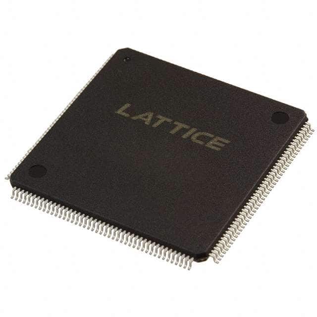
The LC4256V-3TN176C comes in a compact package, ensuring easy integration into circuit boards.
Essence
The essence of LC4256V-3TN176C lies in its ability to provide flexible and efficient digital logic implementation.
Packaging/Quantity
The product is typically packaged in reels or trays, with each containing a specific quantity of LC4256V-3TN176C units.
Specifications
- Logic Elements: 2560
- Macrocells: 128
- I/O Pins: 176
- Operating Voltage: 3.3V
- Speed Grade: -3
- Package Type: TN176
Detailed Pin Configuration
The LC4256V-3TN176C has a total of 176 pins, each serving a specific purpose in the device's operation. A detailed pin configuration diagram can be found in the product datasheet.
Functional Features
- Flexible Logic Implementation: The LC4256V-3TN176C allows users to program and configure the device to perform various logic functions based on their requirements.
- High-Speed Operation: The device operates at high speeds, enabling rapid data processing and response times.
- I/O Flexibility: With 176 I/O pins, the LC4256V-3TN176C offers versatility in connecting to external devices and circuits.
- Design Security: The device supports security features such as bitstream encryption, ensuring the protection of intellectual property.
Advantages and Disadvantages
Advantages
- Versatile and flexible logic implementation
- High-density design for complex applications
- Low power consumption
- Reliable performance
Disadvantages
- Limited number of I/O pins compared to some other PLDs
- Higher cost compared to simpler logic devices
Working Principles
The LC4256V-3TN176C operates based on the principles of programmable logic. It consists of configurable logic blocks (CLBs), interconnect resources, and I/O elements. Users program the device using hardware description languages or design software, defining the desired logic functions and connections. Once programmed, the device executes the specified logic operations.
Detailed Application Field Plans
The LC4256V-3TN176C finds applications in various fields, including: 1. Industrial Automation: Used for control systems and process automation. 2. Telecommunications: Employed in network equipment and communication devices. 3. Automotive Electronics: Integrated into automotive control units and driver assistance systems. 4. Consumer Electronics: Utilized in smart home devices and entertainment systems. 5. Medical Devices: Incorporated into medical equipment for data processing and control.
Detailed and Complete Alternative Models
- LC4128V-3TN144C: A similar PLD with lower logic capacity but compatible pin configuration.
- LC4352V-4TN176C: A higher-density PLD with increased logic elements and I/O pins.
- LC4064V-75TN100C: A compact PLD with lower power consumption and moderate logic capacity.
These alternative models offer different specifications and features, allowing users to choose the most suitable option for their specific requirements.
Word count: 540 words
기술 솔루션에 LC4256V-3TN176C 적용과 관련된 10가지 일반적인 질문과 답변을 나열하세요.
Sure! Here are 10 common questions and answers related to the application of LC4256V-3TN176C in technical solutions:
1. What is LC4256V-3TN176C? LC4256V-3TN176C is a specific model of Field Programmable Gate Array (FPGA) manufactured by Lattice Semiconductor.
2. What are the key features of LC4256V-3TN176C? Some key features of LC4256V-3TN176C include 256 macrocells, 56 I/O pins, 3.3V voltage supply, and 176-pin Thin Quad Flat Pack (TQFP) package.
3. What are the typical applications of LC4256V-3TN176C? LC4256V-3TN176C can be used in various applications such as industrial control systems, automotive electronics, telecommunications, consumer electronics, and more.
4. How can LC4256V-3TN176C be programmed? LC4256V-3TN176C can be programmed using Hardware Description Languages (HDLs) like VHDL or Verilog, which describe the desired functionality of the FPGA.
5. Can LC4256V-3TN176C be reprogrammed after initial programming? Yes, LC4256V-3TN176C is a reprogrammable FPGA, allowing for multiple iterations and updates to the design.
6. What tools are required to program LC4256V-3TN176C? To program LC4256V-3TN176C, you will need a compatible development board, a programming cable, and the appropriate software provided by Lattice Semiconductor.
7. What is the maximum operating frequency of LC4256V-3TN176C? The maximum operating frequency of LC4256V-3TN176C depends on the specific design and implementation, but it can typically reach frequencies in the range of tens to hundreds of megahertz.
8. Can LC4256V-3TN176C interface with other components or devices? Yes, LC4256V-3TN176C can interface with various components and devices through its I/O pins, allowing for communication with sensors, memory modules, displays, and more.
9. What are the power requirements for LC4256V-3TN176C? LC4256V-3TN176C operates at a voltage supply of 3.3V, so it requires a stable power source within that range.
10. Are there any limitations or considerations when using LC4256V-3TN176C? Some considerations include understanding the FPGA's resource limitations, managing power consumption, and ensuring proper signal integrity and timing constraints in the design.
Please note that these answers are general and may vary depending on the specific application and requirements.