

LCMXO2-2000ZE-1UWG49ITRES
Product Overview
Category: Programmable Logic Device (PLD)
Use: The LCMXO2-2000ZE-1UWG49ITRES is a high-performance PLD designed for various digital logic applications. It offers flexibility and versatility in implementing complex logic functions.
Characteristics: - Low power consumption - Small form factor - High-speed performance - Easy to program and reconfigure - Wide range of I/O options
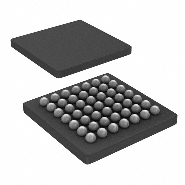
Package: The LCMXO2-2000ZE-1UWG49ITRES comes in a compact 49-ball wafer-level chip-scale package (WLCSP), which allows for space-efficient integration into electronic systems.
Essence: This PLD provides designers with the ability to implement custom logic functions, enabling them to optimize system performance and functionality.
Packaging/Quantity: The LCMXO2-2000ZE-1UWG49ITRES is typically sold in reels or trays, with quantities varying based on customer requirements.
Specifications
- Logic Cells: 2000
- Look-Up Tables (LUTs): 2000
- Flip-Flops: 2000
- Maximum Frequency: 100 MHz
- Operating Voltage: 1.2V
- I/O Voltage: 1.8V / 3.3V
- I/O Standards: LVCMOS, LVTTL, LVDS, SSTL, HSTL
- Package Dimensions: 4.5mm x 4.5mm
Detailed Pin Configuration
The LCMXO2-2000ZE-1UWG49ITRES has a total of 49 pins, each serving a specific purpose. The pin configuration is as follows:
(Pin Number - Pin Name - Function) 1 - VCCIO0 - I/O Power Supply 2 - GND - Ground 3 - IO0 - General Purpose I/O 4 - IO1 - General Purpose I/O 5 - IO2 - General Purpose I/O 6 - IO3 - General Purpose I/O 7 - IO4 - General Purpose I/O 8 - IO5 - General Purpose I/O 9 - IO6 - General Purpose I/O 10 - IO7 - General Purpose I/O 11 - IO8 - General Purpose I/O 12 - IO9 - General Purpose I/O 13 - IO10 - General Purpose I/O 14 - IO11 - General Purpose I/O 15 - IO12 - General Purpose I/O 16 - IO13 - General Purpose I/O 17 - IO14 - General Purpose I/O 18 - IO15 - General Purpose I/O 19 - IO16 - General Purpose I/O 20 - IO17 - General Purpose I/O 21 - IO18 - General Purpose I/O 22 - IO19 - General Purpose I/O 23 - IO20 - General Purpose I/O 24 - IO21 - General Purpose I/O 25 - IO22 - General Purpose I/O 26 - IO23 - General Purpose I/O 27 - IO24 - General Purpose I/O 28 - IO25 - General Purpose I/O 29 - IO26 - General Purpose I/O 30 - IO27 - General Purpose I/O 31 - IO28 - General Purpose I/O 32 - IO29 - General Purpose I/O 33 - IO30 - General Purpose I/O 34 - IO31 - General Purpose I/O 35 - IO32 - General Purpose I/O 36 - IO33 - General Purpose I/O 37 - IO34 - General Purpose I/O 38 - IO35 - General Purpose I/O 39 - IO36 - General Purpose I/O 40 - IO37 - General Purpose I/O 41 - IO38 - General Purpose I/O 42 - IO39 - General Purpose I/O 43 - IO40 - General Purpose I/O 44 - IO41 - General Purpose I/O 45 - IO42 - General Purpose I/O 46 - IO43 - General Purpose I/O 47 - IO44 - General Purpose I/O 48 - IO45 - General Purpose I/O 49 - GND - Ground
Functional Features
- High-speed performance allows for efficient execution of complex logic functions.
- Low power consumption ensures energy efficiency in electronic systems.
- Easy programmability and reconfigurability enable quick design iterations and system modifications.
- Wide range of I/O options provides flexibility in interfacing with other components.
- Compact form factor allows for space-efficient integration into various applications.
Advantages and Disadvantages
기술 솔루션에 LCMXO2-2000ZE-1UWG49ITRES 적용과 관련된 10가지 일반적인 질문과 답변을 나열하세요.
Sure! Here are 10 common questions and answers related to the application of LCMXO2-2000ZE-1UWG49ITRES in technical solutions:
Q1: What is the LCMXO2-2000ZE-1UWG49ITRES? A1: The LCMXO2-2000ZE-1UWG49ITRES is a specific model of Field-Programmable Gate Array (FPGA) manufactured by Lattice Semiconductor.
Q2: What are the key features of the LCMXO2-2000ZE-1UWG49ITRES? A2: Some key features include low power consumption, small form factor, high logic density, and support for various I/O standards.
Q3: What are the typical applications of LCMXO2-2000ZE-1UWG49ITRES? A3: The LCMXO2-2000ZE-1UWG49ITRES is commonly used in applications such as industrial automation, consumer electronics, communication systems, and embedded control systems.
Q4: How does the LCMXO2-2000ZE-1UWG49ITRES help in reducing power consumption? A4: The LCMXO2-2000ZE-1UWG49ITRES utilizes low-power design techniques and offers power management features like clock gating and dynamic power optimization.
Q5: Can the LCMXO2-2000ZE-1UWG49ITRES be programmed after manufacturing? A5: Yes, the LCMXO2-2000ZE-1UWG49ITRES is a programmable device that can be reconfigured even after it has been manufactured.
Q6: What tools are available for programming the LCMXO2-2000ZE-1UWG49ITRES? A6: Lattice Semiconductor provides software tools like Lattice Diamond and iCEcube2 for designing, programming, and debugging the LCMXO2-2000ZE-1UWG49ITRES.
Q7: What are the I/O standards supported by the LCMXO2-2000ZE-1UWG49ITRES? A7: The LCMXO2-2000ZE-1UWG49ITRES supports various I/O standards such as LVCMOS, LVTTL, SSTL, HSTL, LVDS, and more.
Q8: Can the LCMXO2-2000ZE-1UWG49ITRES interface with other components or devices? A8: Yes, the LCMXO2-2000ZE-1UWG49ITRES can interface with other components or devices through its configurable I/O pins.
Q9: Are there any development boards available for prototyping with the LCMXO2-2000ZE-1UWG49ITRES? A9: Yes, Lattice Semiconductor offers development boards like the iCE40 UltraPlus Breakout Board that can be used for prototyping with the LCMXO2-2000ZE-1UWG49ITRES.
Q10: Where can I find more information about the LCMXO2-2000ZE-1UWG49ITRES? A10: You can find more detailed information about the LCMXO2-2000ZE-1UWG49ITRES on the official website of Lattice Semiconductor or by referring to the datasheet and application notes provided by the manufacturer.