

LCMXO2-256HC-5SG32I
Product Overview
Category
The LCMXO2-256HC-5SG32I belongs to the category of Field-Programmable Gate Arrays (FPGAs).
Use
FPGAs are integrated circuits that can be programmed after manufacturing, allowing for flexible and customizable digital logic designs. The LCMXO2-256HC-5SG32I is specifically designed for applications requiring low power consumption and high performance.
Characteristics
- Low power consumption
- High performance
- Programmable logic cells
- Embedded memory blocks
- Flexible I/O options
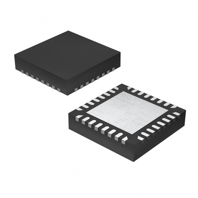
Package
The LCMXO2-256HC-5SG32I comes in a small form factor package, making it suitable for space-constrained applications.
Essence
The essence of the LCMXO2-256HC-5SG32I lies in its ability to provide a versatile and efficient solution for digital logic design, with a focus on low power consumption and high performance.
Packaging/Quantity
The LCMXO2-256HC-5SG32I is typically packaged in trays or reels, with a quantity of 250 units per tray/reel.
Specifications
- Logic Cells: 256
- Speed Grade: -5
- Package Type: SG32
- I/O Pins: 32
- Operating Voltage: 1.2V
- Maximum Frequency: 100 MHz
- Embedded Memory: 4 Kbits
- Configuration Bits: 8,000
Detailed Pin Configuration
The LCMXO2-256HC-5SG32I has a total of 32 I/O pins, which can be configured as inputs or outputs based on the application requirements. The pin configuration is as follows:
- Pin 1: VCCIO
- Pin 2: GND
- Pin 3: IO0
- Pin 4: IO1
- ...
- Pin 32: IO31
Functional Features
Low Power Consumption
The LCMXO2-256HC-5SG32I is designed to operate at low power levels, making it suitable for battery-powered devices and energy-efficient applications.
High Performance
With its high-speed logic cells and embedded memory blocks, the LCMXO2-256HC-5SG32I offers excellent performance for demanding digital logic designs.
Flexible I/O Options
The FPGA provides a range of I/O options, allowing for easy integration with other components and peripherals in the system.
Advantages and Disadvantages
Advantages
- Low power consumption
- High performance
- Programmable flexibility
- Small form factor package
Disadvantages
- Limited logic cell count compared to larger FPGAs
- Limited embedded memory capacity
Working Principles
The LCMXO2-256HC-5SG32I works based on the principle of reconfigurable logic. The programmable logic cells can be interconnected to implement various digital logic functions, while the embedded memory blocks provide additional storage for data processing.
Detailed Application Field Plans
The LCMXO2-256HC-5SG32I finds applications in various fields, including:
- Internet of Things (IoT) devices
- Embedded systems
- Consumer electronics
- Industrial automation
- Communication systems
In these applications, the FPGA's low power consumption, high performance, and flexible I/O options make it an ideal choice for implementing custom digital logic designs.
Detailed and Complete Alternative Models
- LCMXO2-1200HC-4TG100C
- LCMXO2-4000HC-6TG144C
- LCMXO2-7000HC-5TG144C
- LCMXO2-1200ZE-1MG132I
- LCMXO2-4000ZE-3MG132I
These alternative models offer different logic cell counts, package types, and performance characteristics, providing options for various application requirements.
In conclusion, the LCMXO2-256HC-5SG32I is a versatile FPGA that combines low power consumption, high performance, and flexible I/O options. It finds applications in diverse fields and offers several alternative models to cater to different design needs.
기술 솔루션에 LCMXO2-256HC-5SG32I 적용과 관련된 10가지 일반적인 질문과 답변을 나열하세요.
Sure! Here are 10 common questions and answers related to the application of LCMXO2-256HC-5SG32I in technical solutions:
Q: What is the LCMXO2-256HC-5SG32I? A: The LCMXO2-256HC-5SG32I is a low-cost, low-power FPGA (Field-Programmable Gate Array) device manufactured by Lattice Semiconductor.
Q: What are the key features of the LCMXO2-256HC-5SG32I? A: The key features include 256 LUTs (Look-Up Tables), 2,560 flip-flops, 8 multipliers, 32 I/O pins, and support for various I/O standards.
Q: What are some typical applications of the LCMXO2-256HC-5SG32I? A: The LCMXO2-256HC-5SG32I is commonly used in applications such as industrial control systems, consumer electronics, communication devices, and automotive systems.
Q: How can I program the LCMXO2-256HC-5SG32I? A: The LCMXO2-256HC-5SG32I can be programmed using Lattice Diamond or Lattice Radiant software tools, which provide a graphical interface for designing and programming the FPGA.
Q: What voltage levels does the LCMXO2-256HC-5SG32I support? A: The LCMXO2-256HC-5SG32I supports both 3.3V and 1.2V voltage levels, making it compatible with a wide range of digital systems.
Q: Can I use the LCMXO2-256HC-5SG32I in battery-powered applications? A: Yes, the LCMXO2-256HC-5SG32I is designed to be low-power and can be used in battery-powered applications where power consumption is a concern.
Q: Does the LCMXO2-256HC-5SG32I support external memory interfaces? A: No, the LCMXO2-256HC-5SG32I does not have built-in support for external memory interfaces. However, it can be used with external memory controllers if required.
Q: Can I use the LCMXO2-256HC-5SG32I for real-time signal processing? A: Yes, the LCMXO2-256HC-5SG32I's high-speed I/O pins and dedicated multipliers make it suitable for real-time signal processing applications.
Q: What development boards are available for the LCMXO2-256HC-5SG32I? A: Lattice Semiconductor offers various development boards, such as the iCEstick Evaluation Kit, which can be used for prototyping and testing with the LCMXO2-256HC-5SG32I.
Q: Are there any limitations or considerations when using the LCMXO2-256HC-5SG32I? A: Some considerations include limited resources compared to larger FPGAs, limited I/O pins, and the need for external memory controllers if external memory is required. Additionally, complex designs may require higher-capacity FPGAs.