

LCMXO2-256HC-6MG132C
Product Overview
Category
LCMXO2-256HC-6MG132C belongs to the category of Field-Programmable Gate Arrays (FPGAs).
Use
This product is commonly used in electronic circuit design and prototyping. FPGAs provide a flexible platform for implementing digital logic circuits, allowing users to configure the device according to their specific requirements.
Characteristics
- LCMXO2-256HC-6MG132C offers high performance and low power consumption, making it suitable for various applications.
- It provides a large number of configurable logic blocks (CLBs) and programmable interconnects, enabling complex digital designs.
- The device supports various I/O standards, allowing easy integration with other components.
- LCMXO2-256HC-6MG132C offers non-volatile configuration memory, ensuring that the programmed design remains intact even after power loss.
- It has a compact package size, making it suitable for space-constrained applications.
Package and Quantity
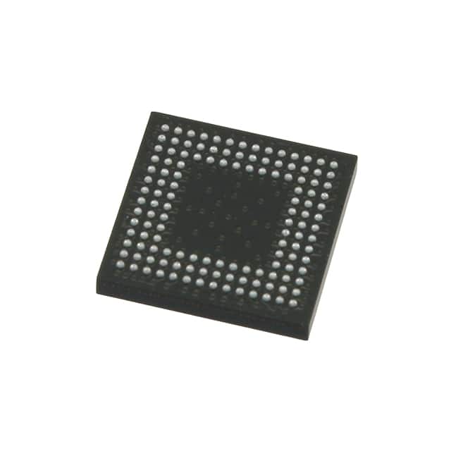
LCMXO2-256HC-6MG132C is available in a 132-pin Quad Flat No-Lead (QFN) package. Each package contains one unit of the FPGA.
Specifications
- Logic Elements: 2560
- Look-Up Tables (LUTs): 2560
- Flip-Flops: 5120
- Block RAM: 64 Kbits
- Maximum User I/Os: 98
- Operating Voltage: 1.2V
- Speed Grade: -6
- Configuration Memory: 256 Kbits
Detailed Pin Configuration
The pin configuration of LCMXO2-256HC-6MG132C is as follows:
- Pin 1: VCCIO
- Pin 2: GND
- Pin 3: IO_0
- Pin 4: IO_1
- ...
- Pin 132: IO_97
Please refer to the product datasheet for a complete pinout diagram.
Functional Features
- LCMXO2-256HC-6MG132C offers reconfigurability, allowing users to modify the design without changing the hardware.
- It supports various clocking options, including global and regional clocks, enabling precise timing control.
- The device provides dedicated hardware resources for implementing arithmetic functions, memory interfaces, and communication protocols.
- LCMXO2-256HC-6MG132C supports partial reconfiguration, allowing specific sections of the design to be modified while the rest remains operational.
Advantages and Disadvantages
Advantages
- High performance and low power consumption
- Flexible and reconfigurable platform
- Compact package size
- Non-volatile configuration memory
Disadvantages
- Limited number of user I/Os
- Steep learning curve for beginners
- Relatively higher cost compared to other programmable logic devices
Working Principles
LCMXO2-256HC-6MG132C operates based on the principles of digital logic. The configurable logic blocks (CLBs) within the FPGA can be programmed to implement various logical functions, such as AND, OR, and XOR gates. These CLBs are interconnected through programmable interconnects, allowing the designer to establish desired connections between different logic elements.
The FPGA is configured by loading a bitstream into its non-volatile configuration memory. This bitstream contains the information required to define the functionality of the FPGA. Once configured, the FPGA executes the programmed logic, performing the desired operations.
Detailed Application Field Plans
LCMXO2-256HC-6MG132C finds applications in various fields, including:
- Embedded Systems: The FPGA can be used to implement complex control systems, communication interfaces, and signal processing algorithms in embedded devices.
- Digital Signal Processing: LCMXO2-256HC-6MG132C can be utilized for implementing digital filters, image processing algorithms, and audio/video codecs.
- Prototyping: The FPGA provides a flexible platform for rapid prototyping of digital circuits, allowing designers to test and validate their designs before manufacturing.
Detailed and Complete Alternative Models
- LCMXO2-1200HC-4TG144C
- LCMXO2-2000HC-5BG256C
- LCMXO2-4000HC-6TG144C
- LCMXO2-7000HC-7TG144C
These alternative models offer different capacities, I/O options, and package sizes, providing flexibility to suit various design requirements.
In conclusion, LCMXO2-256HC-6MG132C is a high-performance FPGA with low power consumption. Its reconfigurability and compact package make it suitable for a wide range of applications in embedded systems, digital signal processing,
기술 솔루션에 LCMXO2-256HC-6MG132C 적용과 관련된 10가지 일반적인 질문과 답변을 나열하세요.
Sure! Here are 10 common questions and answers related to the application of LCMXO2-256HC-6MG132C in technical solutions:
Q: What is the LCMXO2-256HC-6MG132C? A: The LCMXO2-256HC-6MG132C is a low-cost, low-power FPGA (Field-Programmable Gate Array) device manufactured by Lattice Semiconductor.
Q: What are the key features of the LCMXO2-256HC-6MG132C? A: Some key features include 256 LUTs (Look-Up Tables), 128 macrocells, 8Kbits of embedded memory, and support for various I/O standards.
Q: What are some typical applications of the LCMXO2-256HC-6MG132C? A: The LCMXO2-256HC-6MG132C is commonly used in applications such as industrial control systems, consumer electronics, medical devices, and communication equipment.
Q: How can I program the LCMXO2-256HC-6MG132C? A: The LCMXO2-256HC-6MG132C can be programmed using Lattice Diamond or Lattice Radiant software tools, which provide a graphical interface for designing and programming the FPGA.
Q: What voltage levels does the LCMXO2-256HC-6MG132C support? A: The LCMXO2-256HC-6MG132C supports both 3.3V and 1.2V voltage levels, making it compatible with a wide range of digital systems.
Q: Can I use the LCMXO2-256HC-6MG132C in battery-powered applications? A: Yes, the LCMXO2-256HC-6MG132C is designed to be low-power and can be used in battery-powered applications where power efficiency is crucial.
Q: Does the LCMXO2-256HC-6MG132C support any communication protocols? A: Yes, the LCMXO2-256HC-6MG132C supports various communication protocols such as SPI (Serial Peripheral Interface) and I2C (Inter-Integrated Circuit).
Q: Can I use the LCMXO2-256HC-6MG132C for real-time signal processing? A: Yes, the LCMXO2-256HC-6MG132C can be used for real-time signal processing tasks due to its fast logic performance and embedded memory.
Q: Are there any development boards available for the LCMXO2-256HC-6MG132C? A: Yes, Lattice Semiconductor provides development boards like the LCMXO2-256HC-6MG132C-DEMO board, which allows users to prototype and test their designs.
Q: Where can I find documentation and support for the LCMXO2-256HC-6MG132C? A: Documentation, datasheets, application notes, and technical support for the LCMXO2-256HC-6MG132C can be found on the official Lattice Semiconductor website.