

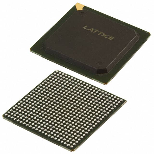
LCMXO2-7000HC-4FG484C
Product Overview
Category
The LCMXO2-7000HC-4FG484C belongs to the category of Field-Programmable Gate Arrays (FPGAs).
Use
FPGAs are integrated circuits that can be programmed or reprogrammed after manufacturing. The LCMXO2-7000HC-4FG484C is specifically designed for use in various electronic systems and applications.
Characteristics
- High capacity: The LCMXO2-7000HC-4FG484C offers a large number of logic cells, making it suitable for complex designs.
- Low power consumption: This FPGA is designed to operate efficiently with minimal power requirements.
- Small form factor: The compact package size allows for easy integration into different electronic devices.
- High-speed performance: The LCMXO2-7000HC-4FG484C offers fast processing capabilities, enabling quick data manipulation.
Package and Quantity
The LCMXO2-7000HC-4FG484C is available in a 484-pin Fine-Pitch Ball Grid Array (FBGA) package. It is typically sold individually or in small quantities.
Specifications
- Logic Cells: 7,000
- Look-Up Tables (LUTs): 4,000
- Flip-Flops: 8,000
- Block RAM: 112 Kbits
- Maximum Operating Frequency: 300 MHz
- I/O Pins: 184
- Voltage Range: 1.14V - 1.26V
- Operating Temperature Range: -40°C to 85°C
Detailed Pin Configuration
The LCMXO2-7000HC-4FG484C has a total of 484 pins. These pins are assigned to various functions such as input/output (I/O), power supply, configuration, and clock signals. A detailed pinout diagram can be found in the product datasheet.
Functional Features
- Programmability: The LCMXO2-7000HC-4FG484C allows users to configure the FPGA according to their specific requirements, enabling customization and flexibility.
- Reconfigurability: The FPGA can be reprogrammed multiple times, allowing for iterative design changes or updates.
- I/O Flexibility: The device offers a range of I/O standards and voltage levels, making it compatible with different interface requirements.
- Embedded Memory: The built-in Block RAM provides on-chip memory resources for data storage and retrieval.
- Low Power Consumption: The LCMXO2-7000HC-4FG484C is designed to operate efficiently, minimizing power consumption.
Advantages and Disadvantages
Advantages
- Versatility: The LCMXO2-7000HC-4FG484C can be used in various applications, including telecommunications, industrial automation, consumer electronics, and more.
- Cost-effective: FPGAs offer a cost-effective solution compared to custom ASICs (Application-Specific Integrated Circuits) for low to medium volume production.
- Rapid Prototyping: FPGAs allow for quick prototyping and development cycles, reducing time-to-market for new products.
- Design Flexibility: The programmable nature of FPGAs enables designers to implement complex logic functions and algorithms.
Disadvantages
- Complexity: Working with FPGAs requires specialized knowledge and expertise in digital design and programming.
- Limited Performance: FPGAs may not match the performance of dedicated hardware solutions for certain high-performance applications.
- Power Consumption: While FPGAs have improved power efficiency, they may still consume more power compared to application-specific solutions.
Working Principles
FPGAs consist of an array of configurable logic blocks interconnected by programmable routing resources. The LCMXO2-7000HC-4FG484C utilizes look-up tables (LUTs) to implement logic functions and flip-flops for sequential circuit elements. The device is programmed using a Hardware Description Language (HDL) such as VHDL or Verilog, which defines the desired functionality of the FPGA.
Detailed Application Field Plans
The LCMXO2-7000HC-4FG484C can be applied in various fields, including:
- Telecommunications: Used in base stations, network switches, and routers for signal processing and protocol handling.
- Industrial Automation: Employed in control systems, motor drives, and robotics for real-time control and monitoring.
- Consumer Electronics: Integrated into smart devices, wearable technology, and multimedia systems for enhanced functionality.
- Automotive: Utilized in advanced driver assistance systems (ADAS), infotainment systems, and engine control units (ECUs).
- Aerospace and Defense: Applied in radar systems, avionics, and secure communication systems for high-reliability applications.
Alternative Models
- LCMXO
기술 솔루션에 LCMXO2-7000HC-4FG484C 적용과 관련된 10가지 일반적인 질문과 답변을 나열하세요.
Sure! Here are 10 common questions and answers related to the application of LCMXO2-7000HC-4FG484C in technical solutions:
Q: What is the LCMXO2-7000HC-4FG484C? A: The LCMXO2-7000HC-4FG484C is a low-cost, low-power FPGA (Field-Programmable Gate Array) device manufactured by Lattice Semiconductor.
Q: What are the key features of the LCMXO2-7000HC-4FG484C? A: Some key features include 7,000 Look-Up Tables (LUTs), 64 Kbits of embedded Block RAM, 58 I/O pins, and support for various I/O standards.
Q: What are some typical applications of the LCMXO2-7000HC-4FG484C? A: It can be used in a wide range of applications such as industrial control systems, consumer electronics, communication devices, and automotive systems.
Q: How can I program the LCMXO2-7000HC-4FG484C? A: The LCMXO2-7000HC-4FG484C can be programmed using Lattice Diamond or Lattice Radiant software tools, which support various programming languages like VHDL and Verilog.
Q: What is the power consumption of the LCMXO2-7000HC-4FG484C? A: The power consumption depends on the design and usage, but typically it operates at low power levels, making it suitable for battery-powered applications.
Q: Can I use the LCMXO2-7000HC-4FG484C in a high-reliability application? A: Yes, the LCMXO2-7000HC-4FG484C is designed to meet high-reliability requirements and can be used in applications where reliability is critical.
Q: Does the LCMXO2-7000HC-4FG484C support external memory interfaces? A: Yes, it supports various memory interfaces such as SPI, I2C, and UART, allowing you to interface with external memory devices.
Q: Can I use the LCMXO2-7000HC-4FG484C for real-time signal processing? A: Yes, the LCMXO2-7000HC-4FG484C has dedicated DSP (Digital Signal Processing) blocks that can be used for real-time signal processing applications.
Q: What are the temperature operating ranges of the LCMXO2-7000HC-4FG484C? A: The LCMXO2-7000HC-4FG484C typically operates within a temperature range of -40°C to 85°C, making it suitable for various environments.
Q: Are there any development boards available for the LCMXO2-7000HC-4FG484C? A: Yes, Lattice Semiconductor provides development boards like the LCMXO2-7000HC-4TG100C or the LCMXO2-7000HE-B-EVN, which can be used for prototyping and evaluation purposes.
Please note that these answers are general and may vary depending on specific design requirements and application scenarios.