

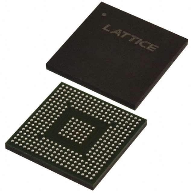
LCMXO2-7000HE-6BG332C
Product Overview
Category
The LCMXO2-7000HE-6BG332C belongs to the category of Field-Programmable Gate Arrays (FPGAs).
Use
This FPGA is commonly used in various electronic applications that require programmable logic functionality.
Characteristics
- High-performance FPGA with low power consumption
- Offers a large number of logic elements and I/O pins
- Provides flexibility for designing complex digital circuits
- Supports reprogramming, allowing for iterative development and testing
Package
The LCMXO2-7000HE-6BG332C comes in a compact Ball Grid Array (BGA) package.
Essence
The essence of this FPGA lies in its ability to provide customizable digital logic functionality, enabling designers to implement their own circuits and algorithms.
Packaging/Quantity
The LCMXO2-7000HE-6BG332C is typically packaged individually and is available in various quantities depending on the supplier.
Specifications
- Logic Elements: 7,000
- Look-Up Tables (LUTs): 4,500
- Flip-Flops: 8,000
- Block RAM: 112 Kbits
- Maximum Operating Frequency: 150 MHz
- I/O Pins: 332
- Voltage Range: 1.14V - 3.465V
- Configuration Memory: 256 Kbits
Detailed Pin Configuration
The LCMXO2-7000HE-6BG332C has a total of 332 I/O pins, each serving a specific purpose in the circuit design. The pin configuration can be found in the manufacturer's datasheet.
Functional Features
- High-performance programmable logic elements
- Flexible I/O capabilities
- On-chip memory blocks for data storage
- Dedicated clock management resources
- Support for various communication protocols
- Built-in security features for protecting intellectual property
Advantages and Disadvantages
Advantages
- Versatile and customizable for a wide range of applications
- Low power consumption, making it suitable for battery-powered devices
- Fast development time due to reprogrammability
- Cost-effective compared to custom ASIC designs
- Availability of development tools and support from the manufacturer
Disadvantages
- Limited performance compared to dedicated hardware implementations
- Higher power consumption compared to specialized ASICs
- Complexity in designing and debugging complex circuits
- Limited availability of alternative models with similar specifications
Working Principles
The LCMXO2-7000HE-6BG332C operates based on the principles of digital logic design. It consists of configurable logic elements, memory blocks, I/O pins, and other supporting resources. The FPGA can be programmed using Hardware Description Languages (HDL) such as VHDL or Verilog. Once programmed, the FPGA executes the desired logic functions by routing signals through its internal components.
Detailed Application Field Plans
The LCMXO2-7000HE-6BG332C finds applications in various fields, including:
- Embedded Systems: Used for implementing custom interfaces, control systems, and signal processing algorithms.
- Communications: Employed in networking equipment, wireless communication devices, and protocol converters.
- Industrial Automation: Utilized for controlling machinery, monitoring sensors, and implementing real-time control systems.
- Consumer Electronics: Integrated into smart devices, gaming consoles, and multimedia systems for enhanced functionality.
- Automotive: Applied in automotive electronics for engine control, driver assistance systems, and infotainment systems.
Detailed and Complete Alternative Models
While the LCMXO2-7000HE-6BG332C offers specific features and specifications, there are alternative FPGA models available from different manufacturers. Some notable alternatives include:
- Xilinx Spartan-6 XC6SLX9: Offers similar logic capacity and I/O capabilities.
- Intel Cyclone IV EP4CE6: Provides comparable performance and power consumption.
- Microchip PolarFire FPGA: Offers higher logic capacity and advanced security features.
These alternative models can be considered based on specific project requirements and design constraints.
Word count: 511 words
기술 솔루션에 LCMXO2-7000HE-6BG332C 적용과 관련된 10가지 일반적인 질문과 답변을 나열하세요.
Sure! Here are 10 common questions and answers related to the application of LCMXO2-7000HE-6BG332C in technical solutions:
Q: What is the LCMXO2-7000HE-6BG332C? A: The LCMXO2-7000HE-6BG332C is a low-cost, low-power FPGA (Field-Programmable Gate Array) device manufactured by Lattice Semiconductor.
Q: What are the key features of the LCMXO2-7000HE-6BG332C? A: Some key features include 7000 Look-Up Tables (LUTs), 128 Kbits of embedded block RAM, 58 I/O pins, and support for various I/O standards.
Q: What are some typical applications of the LCMXO2-7000HE-6BG332C? A: The LCMXO2-7000HE-6BG332C is commonly used in applications such as industrial automation, consumer electronics, medical devices, and communication systems.
Q: How can I program the LCMXO2-7000HE-6BG332C? A: The LCMXO2-7000HE-6BG332C can be programmed using Lattice Diamond or Lattice Radiant software tools, which support various programming languages like VHDL and Verilog.
Q: What is the power consumption of the LCMXO2-7000HE-6BG332C? A: The LCMXO2-7000HE-6BG332C has low power consumption, typically ranging from 25 to 150 milliwatts depending on the operating conditions.
Q: Can I use the LCMXO2-7000HE-6BG332C in battery-powered devices? A: Yes, the low power consumption of the LCMXO2-7000HE-6BG332C makes it suitable for battery-powered applications where power efficiency is crucial.
Q: Does the LCMXO2-7000HE-6BG332C support communication interfaces like UART or SPI? A: Yes, the LCMXO2-7000HE-6BG332C supports various communication interfaces, including UART, SPI, I2C, and GPIO.
Q: Can I use the LCMXO2-7000HE-6BG332C for real-time signal processing? A: Yes, the LCMXO2-7000HE-6BG332C can be used for real-time signal processing tasks due to its high-speed performance and dedicated DSP (Digital Signal Processing) blocks.
Q: What are the temperature operating ranges for the LCMXO2-7000HE-6BG332C? A: The LCMXO2-7000HE-6BG332C has a commercial temperature range of 0°C to 85°C and an industrial temperature range of -40°C to 100°C.
Q: Are there any development boards available for the LCMXO2-7000HE-6BG332C? A: Yes, Lattice Semiconductor provides development boards like the LCMXO2-7000HE-B-EVN, which allow users to prototype and test their designs using the LCMXO2-7000HE-6BG332C FPGA.
Please note that the answers provided here are general and may vary depending on specific requirements and use cases.