

LCMXO3LF-6900C-6BG324I
Product Overview
Category: Programmable Logic Device (PLD)
Use: The LCMXO3LF-6900C-6BG324I is a high-performance PLD designed for various digital logic applications. It offers flexibility and versatility in implementing complex logic functions.
Characteristics: - Low power consumption - High-speed performance - Small form factor - Easy to program and reconfigure - Wide operating temperature range
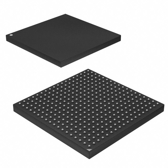
Package: The LCMXO3LF-6900C-6BG324I comes in a 324-ball grid array (BGA) package, which provides excellent electrical and thermal properties.
Essence: This PLD is based on the Lattice Semiconductor's MachXO3LF family, known for its low-power and high-density characteristics. It combines programmable logic and embedded memory resources to enable efficient implementation of digital designs.
Packaging/Quantity: The LCMXO3LF-6900C-6BG324I is typically sold individually or in reels, with quantities varying based on customer requirements.
Specifications
- Logic Elements: 6,900
- Look-Up Tables (LUTs): 4,500
- Embedded Block RAM: 270 Kbits
- User Flash Memory: 64 Kbits
- I/O Pins: 324
- Operating Voltage: 1.2V
- Maximum Frequency: 300 MHz
- Package Dimensions: 17mm x 17mm
Detailed Pin Configuration
The LCMXO3LF-6900C-6BG324I has a total of 324 pins, each serving a specific purpose. The pin configuration includes dedicated input/output pins, clock inputs, power supply pins, and configuration interface pins. For a detailed pinout diagram and description, refer to the product datasheet.
Functional Features
- Programmable logic resources for implementing complex digital designs
- Embedded memory blocks for efficient data storage and retrieval
- Flexible I/O capabilities for interfacing with external devices
- Low-power operation for energy-efficient applications
- High-speed performance for time-critical operations
- Easy programming and reconfiguration using industry-standard design tools
Advantages and Disadvantages
Advantages: - Low power consumption makes it suitable for battery-powered devices - High-density logic elements allow for complex designs in a small footprint - Versatile I/O options enable seamless integration with various peripherals - Easy-to-use design tools simplify the development process - Wide operating temperature range ensures reliability in harsh environments
Disadvantages: - Limited availability of alternative models from other manufacturers - Higher cost compared to some competing PLDs - Steeper learning curve for beginners due to its advanced features
Working Principles
The LCMXO3LF-6900C-6BG324I operates based on the principles of programmable logic. It consists of configurable logic blocks (CLBs) that can be interconnected to implement desired logic functions. The device is programmed using hardware description languages (HDLs) or schematic entry tools, which generate a configuration bitstream. This bitstream is then loaded into the PLD, configuring it to perform the desired logic operations.
Detailed Application Field Plans
The LCMXO3LF-6900C-6BG324I finds applications in various fields, including: 1. Industrial automation: Control systems, motor drives, and sensor interfaces. 2. Communications: Data routers, network switches, and protocol converters. 3. Consumer electronics: Smart home devices, wearable technology, and gaming consoles. 4. Automotive: Infotainment systems, driver assistance, and engine control units. 5. Aerospace and defense: Avionics, radar systems, and secure communication devices.
Detailed and Complete Alternative Models
While the LCMXO3LF-6900C-6BG324I is a highly capable PLD, there are alternative models available from other manufacturers. Some notable alternatives include: - Xilinx Spartan-7 series - Intel (formerly Altera) MAX 10 series - Microchip PolarFire series
These alternative models offer similar functionality and can be considered based on specific project requirements.
In conclusion, the LCMXO3LF-6900C-6BG324I is a versatile and high-performance programmable logic device suitable for a wide range of digital logic applications. Its low power consumption, small form factor, and flexible I/O capabilities make it an attractive choice for designers seeking efficient and reliable solutions.
기술 솔루션에 LCMXO3LF-6900C-6BG324I 적용과 관련된 10가지 일반적인 질문과 답변을 나열하세요.
Sure! Here are 10 common questions and answers related to the application of LCMXO3LF-6900C-6BG324I in technical solutions:
Q: What is the LCMXO3LF-6900C-6BG324I? A: The LCMXO3LF-6900C-6BG324I is a specific model of Field-Programmable Gate Array (FPGA) manufactured by Lattice Semiconductor.
Q: What are the key features of the LCMXO3LF-6900C-6BG324I? A: Some key features include low power consumption, small form factor, high-performance logic fabric, and embedded memory blocks.
Q: In what applications can the LCMXO3LF-6900C-6BG324I be used? A: It can be used in various applications such as industrial automation, automotive electronics, consumer electronics, telecommunications, and more.
Q: How does the LCMXO3LF-6900C-6BG324I help in industrial automation? A: It can be used for tasks like motor control, sensor interfacing, data acquisition, and implementing complex control algorithms.
Q: Can the LCMXO3LF-6900C-6BG324I be used in automotive electronics? A: Yes, it can be used for applications like advanced driver-assistance systems (ADAS), infotainment systems, engine control units (ECUs), and more.
Q: What advantages does the LCMXO3LF-6900C-6BG324I offer in consumer electronics? A: It provides flexibility, allowing designers to implement custom functionality, accelerate time-to-market, and reduce overall system cost.
Q: How can the LCMXO3LF-6900C-6BG324I be used in telecommunications? A: It can be used for tasks like protocol conversion, signal processing, encryption/decryption, and implementing custom communication interfaces.
Q: Does the LCMXO3LF-6900C-6BG324I support high-speed data transfer? A: Yes, it supports high-speed I/O standards such as LVDS, DDR, and SERDES, enabling fast data transfer rates.
Q: Can the LCMXO3LF-6900C-6BG324I be reprogrammed after deployment? A: Yes, it is a field-programmable device, allowing for easy updates and modifications to the implemented logic.
Q: What development tools are available for working with the LCMXO3LF-6900C-6BG324I? A: Lattice Semiconductor provides software tools like Lattice Diamond, Lattice Radiant, and Lattice Propel for designing, programming, and debugging FPGA designs.
Please note that the specific applications and features mentioned above are just examples, and the LCMXO3LF-6900C-6BG324I can be used in many other technical solutions depending on the requirements.