

LFE2-70E-5FN672I
Product Overview
Category
The LFE2-70E-5FN672I belongs to the category of Field Programmable Gate Arrays (FPGAs).
Use
This FPGA is commonly used in various electronic devices and systems for digital logic implementation, such as communication equipment, industrial control systems, and consumer electronics.
Characteristics
- High flexibility: The LFE2-70E-5FN672I offers a high level of programmability, allowing users to configure the device according to their specific requirements.
- Large capacity: With its 70,000 logic elements, this FPGA provides ample resources for complex digital designs.
- Low power consumption: The LFE2-70E-5FN672I is designed to operate efficiently with low power consumption, making it suitable for battery-powered applications.
- Fast performance: This FPGA offers high-speed operation, enabling rapid data processing and real-time applications.
Package and Quantity
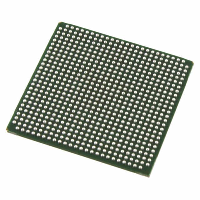
The LFE2-70E-5FN672I comes in a compact package, measuring 672-ball FineLine BGA. It is typically sold individually or in small quantities.
Specifications
- Logic Elements: 70,000
- Embedded Memory: Up to 1,152 Kbits
- I/O Pins: 672
- Operating Voltage: 1.2V
- Maximum Frequency: 400 MHz
- Configuration Memory: Flash-based
Detailed Pin Configuration
For detailed pin configuration information, please refer to the manufacturer's datasheet or user manual.
Functional Features
- High-speed serial transceivers: The LFE2-70E-5FN672I includes multiple high-speed serial transceivers, enabling fast data transfer between devices.
- Flexible I/O interfaces: This FPGA supports various I/O standards, allowing seamless integration with different external components.
- On-chip memory: The embedded memory blocks provide additional storage for data processing and temporary storage requirements.
- Clock management: The device offers advanced clocking features, including PLLs and DLLs, to ensure precise timing control.
Advantages
- Versatility: The LFE2-70E-5FN672I can be programmed to perform a wide range of functions, making it suitable for diverse applications.
- Scalability: With its large logic capacity, this FPGA can accommodate complex designs and future expansion needs.
- Power efficiency: The low power consumption of the LFE2-70E-5FN672I contributes to energy-efficient system operation.
- High performance: The FPGA's fast processing capabilities enable efficient execution of complex algorithms and real-time tasks.
Disadvantages
- Learning curve: Utilizing FPGAs requires specialized knowledge and expertise in digital design and programming.
- Cost: FPGAs tend to be more expensive compared to other integrated circuits due to their programmable nature and advanced features.
Working Principles
The LFE2-70E-5FN672I operates based on the principles of reconfigurable digital logic. It consists of an array of configurable logic elements interconnected through programmable routing resources. Users can program the FPGA by defining the desired logic functions and interconnections using Hardware Description Languages (HDLs) like VHDL or Verilog. Once programmed, the FPGA executes the specified logic operations, enabling the desired functionality.
Detailed Application Field Plans
The LFE2-70E-5FN672I finds applications in various fields, including: 1. Communication Systems: Used for protocol conversion, signal processing, and encryption/decryption tasks. 2. Industrial Control Systems: Employed in automation, motor control, and sensor interfacing applications. 3. Consumer Electronics: Integrated into multimedia devices, gaming consoles, and high-performance audio/video systems. 4. Medical Equipment: Utilized for image processing, patient monitoring, and diagnostic systems. 5. Aerospace and Defense: Applied in radar systems, avionics, and secure communication equipment.
Detailed Alternative Models
- LFE2-35E-4FN672C
- LFE2-200E-6FN672I
- LFE3-95EA-8FN672C
- LFE5U-85F-8BG756I
These alternative models offer varying logic capacities, I/O pin counts, and additional features to cater to different design requirements.
In conclusion, the LFE2-70E-5FN672I is a versatile FPGA with high flexibility, large capacity, and low power consumption. Its functional features, advantages, and disadvantages make it suitable for a wide range of applications in various fields.
기술 솔루션에 LFE2-70E-5FN672I 적용과 관련된 10가지 일반적인 질문과 답변을 나열하세요.
Sure! Here are 10 common questions and answers related to the application of LFE2-70E-5FN672I in technical solutions:
Q: What is the LFE2-70E-5FN672I? A: The LFE2-70E-5FN672I is a specific model of Field-Programmable Gate Array (FPGA) manufactured by Lattice Semiconductor.
Q: What are the key features of the LFE2-70E-5FN672I? A: The key features of this FPGA include 70,000 Look-Up Tables (LUTs), 672-pin FineLine BGA package, low power consumption, and high-speed performance.
Q: In what applications can the LFE2-70E-5FN672I be used? A: This FPGA can be used in various applications such as telecommunications, industrial automation, automotive electronics, medical devices, and consumer electronics.
Q: What advantages does the LFE2-70E-5FN672I offer over other FPGAs? A: Some advantages of this FPGA include its low power consumption, high-speed performance, large number of LUTs for complex designs, and availability of various I/O interfaces.
Q: How can I program the LFE2-70E-5FN672I? A: The LFE2-70E-5FN672I can be programmed using Lattice Diamond design software or other compatible programming tools provided by Lattice Semiconductor.
Q: Can I use the LFE2-70E-5FN672I for real-time signal processing? A: Yes, the LFE2-70E-5FN672I is capable of real-time signal processing due to its high-speed performance and large number of LUTs.
Q: What is the power supply requirement for the LFE2-70E-5FN672I? A: The LFE2-70E-5FN672I requires a power supply voltage of 1.2V, which can be provided by an external power source.
Q: Does the LFE2-70E-5FN672I support different I/O standards? A: Yes, this FPGA supports various I/O standards such as LVCMOS, LVTTL, LVDS, SSTL, and HSTL, making it compatible with different interface requirements.
Q: Can I use the LFE2-70E-5FN672I in high-reliability applications? A: Yes, the LFE2-70E-5FN672I is suitable for high-reliability applications as it offers robust design features and is manufactured using reliable processes.
Q: Where can I find more information about the LFE2-70E-5FN672I? A: You can find more detailed information about the LFE2-70E-5FN672I, including datasheets, application notes, and reference designs, on the official website of Lattice Semiconductor or by contacting their technical support team.