

LFE2-70SE-6FN900C
Product Overview
Category
The LFE2-70SE-6FN900C belongs to the category of Field Programmable Gate Arrays (FPGAs).
Use
This FPGA is commonly used in electronic circuits for various applications, including digital signal processing, telecommunications, and embedded systems.
Characteristics
- High-performance FPGA with advanced features
- Low power consumption
- Flexible and reconfigurable design
- Suitable for complex logic implementations
- Offers high-speed data processing capabilities
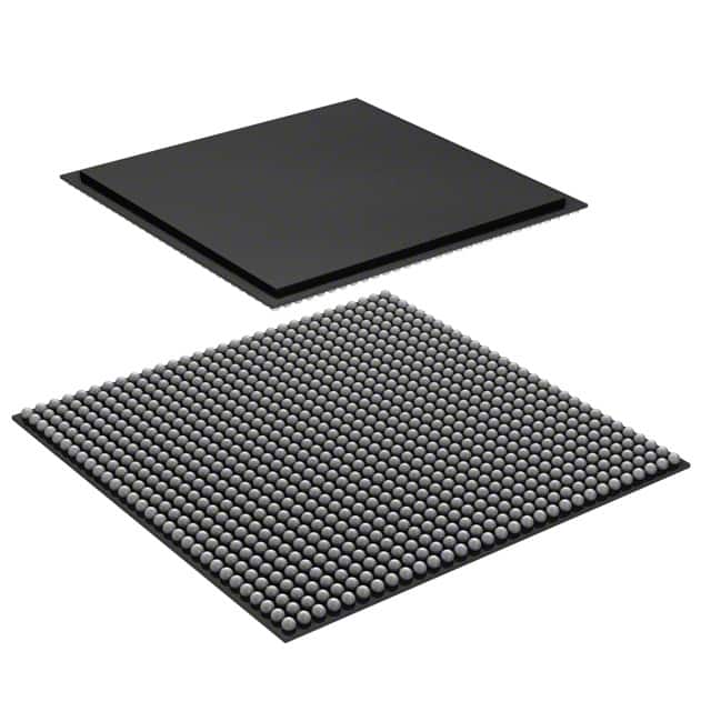
Package
The LFE2-70SE-6FN900C comes in a compact package that ensures easy integration into electronic circuit boards.
Essence
The essence of the LFE2-70SE-6FN900C lies in its ability to provide a customizable and versatile solution for implementing complex digital logic designs.
Packaging/Quantity
This FPGA is typically packaged individually and is available in various quantities depending on the specific requirements of the user or project.
Specifications
- Model: LFE2-70SE-6FN900C
- Logic Elements: 70,000
- Speed Grade: 6
- Number of I/O Pins: 900
- Operating Voltage: 1.2V
- Package Type: FN900C
Detailed Pin Configuration
The LFE2-70SE-6FN900C has a comprehensive pin configuration that allows for seamless integration into electronic circuits. The detailed pin configuration can be found in the product datasheet provided by the manufacturer.
Functional Features
- High-speed data processing capabilities
- Configurable logic elements for custom designs
- On-chip memory blocks for efficient data storage
- Built-in multipliers for arithmetic operations
- Support for various communication protocols
- Integrated clock management resources
Advantages and Disadvantages
Advantages
- Versatile and customizable design
- Low power consumption
- High-performance capabilities
- Suitable for complex logic implementations
- Wide range of I/O pins for connectivity options
Disadvantages
- Steep learning curve for beginners
- Higher cost compared to simpler programmable logic devices
- Limited availability of alternative models with similar specifications
Working Principles
The LFE2-70SE-6FN900C operates based on the principles of field-programmable gate arrays. It consists of configurable logic elements, memory blocks, and other resources that can be programmed to implement desired digital logic designs. The FPGA is typically programmed using a hardware description language (HDL) and then loaded onto the device for execution.
Detailed Application Field Plans
The LFE2-70SE-6FN900C finds applications in various fields, including:
- Digital Signal Processing: Used for implementing complex algorithms and signal processing tasks in areas such as audio and video processing, image recognition, and data compression.
- Telecommunications: Employed in communication systems for tasks like protocol handling, encryption/decryption, and error correction.
- Embedded Systems: Integrated into embedded systems for controlling and managing various functions, such as motor control, sensor interfacing, and user interface implementation.
Detailed and Complete Alternative Models
While the LFE2-70SE-6FN900C offers advanced features and performance, there are alternative FPGA models available in the market with similar capabilities. Some notable alternatives include:
- Xilinx Virtex UltraScale+: Offers high-performance capabilities and advanced features suitable for complex designs.
- Intel Stratix 10: Provides a wide range of resources and high-speed interfaces for demanding applications.
- Microsemi SmartFusion2: Combines FPGA fabric with microcontroller capabilities, making it suitable for mixed-signal applications.
These alternative models offer different trade-offs in terms of performance, power consumption, and pricing, allowing users to choose the most suitable option for their specific requirements.
In conclusion, the LFE2-70SE-6FN900C is a high-performance FPGA that offers flexibility, versatility, and advanced features for implementing complex digital logic designs. Its wide range of applications and availability of alternative models make it a valuable component in various electronic systems.
기술 솔루션에 LFE2-70SE-6FN900C 적용과 관련된 10가지 일반적인 질문과 답변을 나열하세요.
Sure! Here are 10 common questions and answers related to the application of LFE2-70SE-6FN900C in technical solutions:
Q: What is the LFE2-70SE-6FN900C? A: The LFE2-70SE-6FN900C is a specific model of Field-Programmable Gate Array (FPGA) manufactured by Lattice Semiconductor.
Q: What are the key features of the LFE2-70SE-6FN900C? A: The key features of this FPGA include 70,000 Look-Up Tables (LUTs), 900 MHz maximum operating frequency, and support for various I/O standards.
Q: In what applications can the LFE2-70SE-6FN900C be used? A: This FPGA can be used in a wide range of applications such as telecommunications, industrial automation, automotive electronics, and medical devices.
Q: How can I program the LFE2-70SE-6FN900C? A: The LFE2-70SE-6FN900C can be programmed using hardware description languages (HDLs) like VHDL or Verilog, along with design software provided by Lattice Semiconductor.
Q: What are the power requirements for the LFE2-70SE-6FN900C? A: The LFE2-70SE-6FN900C typically requires a supply voltage of 1.2V and consumes power based on the complexity of the design and operating frequency.
Q: Can I interface the LFE2-70SE-6FN900C with other components or peripherals? A: Yes, the LFE2-70SE-6FN900C supports various I/O standards, allowing it to interface with other components such as sensors, memory devices, and communication modules.
Q: What are the advantages of using the LFE2-70SE-6FN900C in my design? A: The advantages include its high logic capacity, fast operating frequency, flexibility for customization, and ability to implement complex digital designs.
Q: Are there any limitations or considerations when using the LFE2-70SE-6FN900C? A: Some considerations include power consumption, heat dissipation, and the need for proper signal integrity and timing analysis during the design phase.
Q: Can I reprogram the LFE2-70SE-6FN900C after it has been deployed in a system? A: Yes, FPGAs like the LFE2-70SE-6FN900C can be reprogrammed multiple times, allowing for design updates or changes without replacing the hardware.
Q: Where can I find additional resources and support for the LFE2-70SE-6FN900C? A: You can refer to the official documentation, datasheets, application notes, and online forums provided by Lattice Semiconductor for further information and technical support.
Please note that the specific details and answers may vary based on the manufacturer's specifications and documentation.