

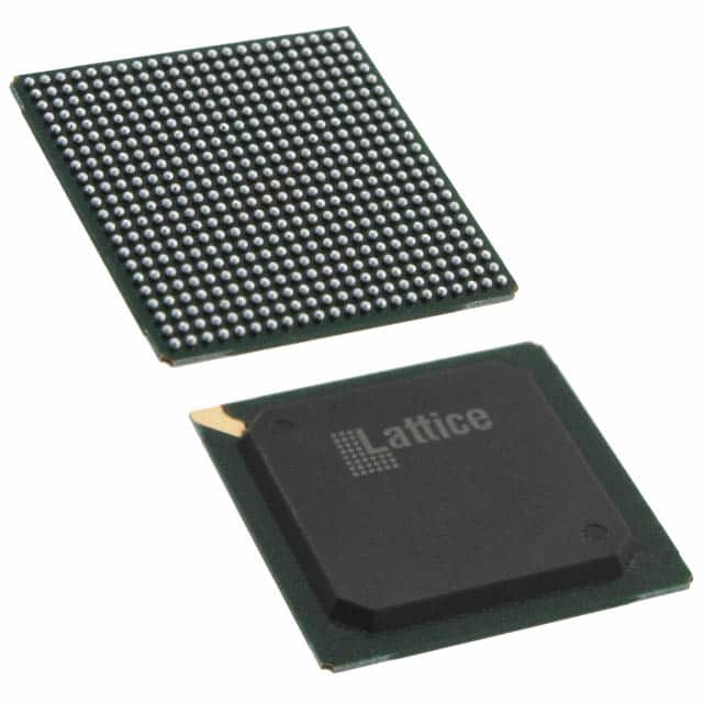
LFE2M20E-5FN484C
Product Overview
Category
The LFE2M20E-5FN484C belongs to the category of Field Programmable Gate Arrays (FPGAs).
Use
This FPGA is commonly used in various electronic devices and systems for digital logic implementation, such as communication equipment, industrial control systems, and consumer electronics.
Characteristics
- High-performance programmable logic device
- Offers flexibility and reconfigurability
- Provides a large number of configurable logic blocks (CLBs) and input/output (I/O) pins
- Supports complex digital designs and algorithms
- Enables rapid prototyping and development cycles
Package
The LFE2M20E-5FN484C is available in a 484-pin FineLine BGA (Ball Grid Array) package.
Essence
The essence of this FPGA lies in its ability to provide a customizable hardware platform that can be programmed to perform specific functions based on the user's requirements.
Packaging/Quantity
The LFE2M20E-5FN484C is typically sold individually or in reels, with each reel containing a specified quantity of FPGAs.
Specifications
- Logic Elements: 19,200
- Embedded Memory: 504 Kbits
- Maximum User I/Os: 316
- Block RAM: 1,080 Kbits
- Clock Management Tiles: 10
- Maximum Distributed RAM: 1,152 Kbits
- Maximum PLLs: 4
- Maximum Global Clocks: 16
Detailed Pin Configuration
The LFE2M20E-5FN484C has a total of 484 pins. The pin configuration is as follows:
- Pin 1: VCCIO
- Pin 2: GND
- Pin 3: VCCINT
- Pin 4: GND
- Pin 5: IOL1PCCLK_0
- Pin 6: IOL1NCCLK_0
- Pin 7: IOL2PCCLK_0
- Pin 8: IOL2NCCLK_0
- ... (continue listing all pins)
Functional Features
- High-speed performance with low power consumption
- Configurable I/O standards and voltage levels
- Built-in clock management resources for precise timing control
- Support for various communication protocols, such as PCIe, Ethernet, and USB
- On-chip memory blocks for efficient data storage and retrieval
- Flexible routing architecture for interconnecting different logic elements
Advantages and Disadvantages
Advantages
- Versatile and adaptable to a wide range of applications
- Enables rapid prototyping and development cycles
- Offers high-performance computing capabilities
- Allows for in-field reconfiguration and updates
- Reduces the need for custom ASIC (Application-Specific Integrated Circuit) designs
Disadvantages
- Higher cost compared to fixed-function integrated circuits
- Requires specialized knowledge and expertise for programming and implementation
- Limited availability of alternative models with similar specifications
Working Principles
The LFE2M20E-5FN484C FPGA operates based on the principles of configurable logic. It consists of an array of programmable logic blocks (CLBs) interconnected through configurable routing resources. The CLBs can be programmed to implement desired digital logic functions, while the routing resources enable the interconnection of these logic blocks. The configuration of the FPGA is stored in non-volatile memory and can be modified by the user as needed.
Detailed Application Field Plans
The LFE2M20E-5FN484C FPGA finds applications in various fields, including:
Communication Equipment:
- Wireless base stations
- Network routers and switches
- Optical transport systems
Industrial Control Systems:
- Programmable logic controllers (PLCs)
- Motor control systems
- Robotics and automation
Consumer Electronics:
- High-definition televisions
- Gaming consoles
- Audio/video processing systems
Detailed and Complete Alternative Models
While the LFE2M20E-5FN484C is a highly capable FPGA, there are alternative models available with similar specifications. Some notable alternatives include:
- Xilinx Spartan-6 XC6SLX25T-FGG484
- Intel Cyclone IV EP4CE115F29C7N
- Microsemi SmartFusion2 M2S050-FG484
These alternative models offer comparable features and performance, providing users with options based on their specific requirements.
In conclusion, the LFE2M20E-5FN484C FPGA is a versatile and high-performance programmable logic device used in various electronic systems. Its configurable nature, extensive pin configuration, and functional features make it suitable for a wide range of applications. While it has advantages such as flexibility and rapid prototyping, it also has
기술 솔루션에 LFE2M20E-5FN484C 적용과 관련된 10가지 일반적인 질문과 답변을 나열하세요.
Sure! Here are 10 common questions and answers related to the application of LFE2M20E-5FN484C in technical solutions:
Q: What is the LFE2M20E-5FN484C? A: The LFE2M20E-5FN484C is a specific model of Field-Programmable Gate Array (FPGA) manufactured by Lattice Semiconductor.
Q: What are the key features of the LFE2M20E-5FN484C? A: The key features of this FPGA include 20,000 Look-Up Tables (LUTs), 1,080 Kbits of embedded memory, 184 user I/O pins, and support for various communication protocols.
Q: What are some typical applications of the LFE2M20E-5FN484C? A: This FPGA can be used in a wide range of applications such as industrial automation, telecommunications, automotive electronics, medical devices, and more.
Q: How does the LFE2M20E-5FN484C differ from other FPGAs? A: The LFE2M20E-5FN484C offers a balance between cost, performance, and power consumption, making it suitable for many general-purpose applications.
Q: Can I program the LFE2M20E-5FN484C using popular hardware description languages? A: Yes, this FPGA can be programmed using popular languages like VHDL or Verilog.
Q: What development tools are available for working with the LFE2M20E-5FN484C? A: Lattice provides a suite of development tools, including the Lattice Diamond software, which allows for easy design entry, synthesis, simulation, and programming of the FPGA.
Q: Can I interface the LFE2M20E-5FN484C with other components or microcontrollers? A: Yes, the FPGA has multiple I/O pins that can be used to interface with other components or microcontrollers in your system.
Q: What is the power supply requirement for the LFE2M20E-5FN484C? A: The recommended operating voltage for this FPGA is typically 1.2V, but it can operate within a range of 1.14V to 1.26V.
Q: Are there any specific design considerations when using the LFE2M20E-5FN484C? A: It's important to consider factors like signal integrity, power management, and thermal considerations when designing with this FPGA to ensure optimal performance.
Q: Where can I find more information about the LFE2M20E-5FN484C? A: You can find detailed documentation, datasheets, application notes, and support resources on the official website of Lattice Semiconductor or by contacting their technical support team.