

LFE3-70EA-7FN672I
Product Overview
Category
The LFE3-70EA-7FN672I belongs to the category of Field Programmable Gate Arrays (FPGAs).
Use
This FPGA is commonly used in electronic systems for various applications such as telecommunications, automotive, aerospace, and industrial control.
Characteristics
- High-performance programmable logic device
- Offers high-speed data processing capabilities
- Provides flexibility for system customization
- Supports complex digital circuit designs
- Enables rapid prototyping and development
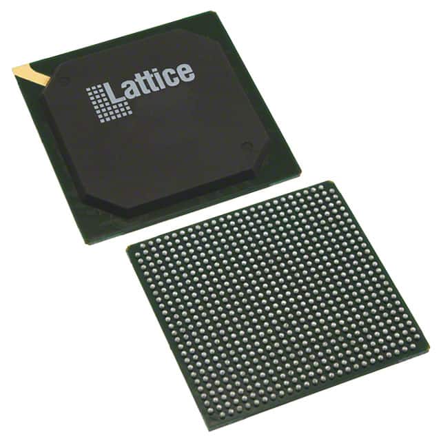
Package
The LFE3-70EA-7FN672I comes in a compact and durable package that ensures protection during handling and installation.
Essence
The essence of this FPGA lies in its ability to provide a versatile platform for implementing complex digital circuits with high performance and flexibility.
Packaging/Quantity
Each package of LFE3-70EA-7FN672I contains one unit of the FPGA.
Specifications
- Device Type: Field Programmable Gate Array (FPGA)
- Model: LFE3-70EA-7FN672I
- Logic Elements: 70,000
- Number of Pins: 672
- Operating Voltage: 1.2V
- Maximum Frequency: 500 MHz
- Configuration Memory: 4 Mb
- I/O Standards: LVCMOS, LVTTL, SSTL, HSTL, LVDS, RSDS
Detailed Pin Configuration
The LFE3-70EA-7FN672I has a total of 672 pins, each serving a specific purpose in the overall functionality of the FPGA. The detailed pin configuration can be found in the product datasheet provided by the manufacturer.
Functional Features
- High-speed data processing capabilities
- Configurable logic elements for custom circuit implementation
- Embedded memory blocks for efficient data storage
- Flexible I/O standards for seamless integration with other components
- Built-in clock management resources for precise timing control
Advantages and Disadvantages
Advantages
- High-performance FPGA suitable for demanding applications
- Versatile platform for rapid prototyping and development
- Customizable logic elements for tailored circuit designs
- Wide range of supported I/O standards for compatibility
- Efficient use of embedded memory blocks
Disadvantages
- Relatively high power consumption compared to other programmable logic devices
- Steeper learning curve for beginners due to the complexity of FPGA programming
- Higher cost compared to simpler programmable logic devices
Working Principles
The LFE3-70EA-7FN672I operates based on the principles of reconfigurable digital logic. It consists of configurable logic elements, embedded memory blocks, and various I/O interfaces. The FPGA can be programmed using hardware description languages (HDLs) such as VHDL or Verilog. Once programmed, the FPGA executes the desired digital circuit functionality by routing signals through its configurable logic elements.
Detailed Application Field Plans
The LFE3-70EA-7FN672I finds extensive application in various fields, including:
- Telecommunications: Used in network routers, switches, and communication equipment for high-speed data processing.
- Automotive: Employed in automotive electronics for advanced driver assistance systems (ADAS), engine control units (ECUs), and infotainment systems.
- Aerospace: Utilized in avionics systems for flight control, navigation, and communication.
- Industrial Control: Integrated into industrial automation systems for process control, monitoring, and robotics.
Detailed and Complete Alternative Models
- LFE3-35EA-6FN484C: A lower-capacity FPGA with 35,000 logic elements and 484 pins.
- LFE5UM-85F-8BG756I: A higher-capacity FPGA with 85,000 logic elements and 756 pins.
- LFE5UM-45F-8MG285C: A mid-range FPGA with 45,000 logic elements and 285 pins.
These alternative models offer different capacity and pin configurations to cater to specific project requirements.
Word count: 470 words
기술 솔루션에 LFE3-70EA-7FN672I 적용과 관련된 10가지 일반적인 질문과 답변을 나열하세요.
Sure! Here are 10 common questions and answers related to the application of LFE3-70EA-7FN672I in technical solutions:
Q: What is the LFE3-70EA-7FN672I? A: The LFE3-70EA-7FN672I is a field-programmable gate array (FPGA) manufactured by Lattice Semiconductor.
Q: What are the key features of the LFE3-70EA-7FN672I? A: Some key features include 70,000 Look-Up Tables (LUTs), high-speed I/O interfaces, embedded memory blocks, and low power consumption.
Q: In what applications can the LFE3-70EA-7FN672I be used? A: The LFE3-70EA-7FN672I can be used in various applications such as telecommunications, industrial automation, automotive electronics, and medical devices.
Q: How can I program the LFE3-70EA-7FN672I? A: The LFE3-70EA-7FN672I can be programmed using hardware description languages (HDLs) like VHDL or Verilog, or through graphical programming tools provided by Lattice Semiconductor.
Q: What is the maximum operating frequency of the LFE3-70EA-7FN672I? A: The maximum operating frequency of the LFE3-70EA-7FN672I depends on the specific design and implementation, but it can typically reach several hundred megahertz (MHz).
Q: Can the LFE3-70EA-7FN672I interface with other components or devices? A: Yes, the LFE3-70EA-7FN672I supports various communication protocols such as SPI, I2C, UART, and Ethernet, allowing it to interface with other components or devices.
Q: What are the power requirements for the LFE3-70EA-7FN672I? A: The LFE3-70EA-7FN672I operates at a voltage range of 1.2V to 3.3V, with power consumption depending on the specific design and usage.
Q: Can the LFE3-70EA-7FN672I be used in safety-critical applications? A: Yes, the LFE3-70EA-7FN672I can be used in safety-critical applications as it supports various reliability features like error correction codes (ECC) and built-in self-test (BIST) capabilities.
Q: Are there any development tools available for the LFE3-70EA-7FN672I? A: Yes, Lattice Semiconductor provides development tools like Lattice Diamond and Lattice Radiant, which offer design entry, synthesis, simulation, and programming capabilities.
Q: Where can I find more information about the LFE3-70EA-7FN672I? A: You can find more detailed information about the LFE3-70EA-7FN672I, including datasheets, application notes, and reference designs, on the official website of Lattice Semiconductor.