

LFE5U-85F-7BG756I
Product Overview
Category
The LFE5U-85F-7BG756I belongs to the category of Field Programmable Gate Arrays (FPGAs).
Use
This FPGA is designed for various applications that require high-performance and flexible digital logic circuits. It provides a customizable hardware platform that can be programmed to perform specific tasks.
Characteristics
- High-performance FPGA with advanced features
- Flexible and reprogrammable design
- Supports complex digital logic functions
- Offers high-speed data processing capabilities
- Low power consumption
- Suitable for a wide range of applications
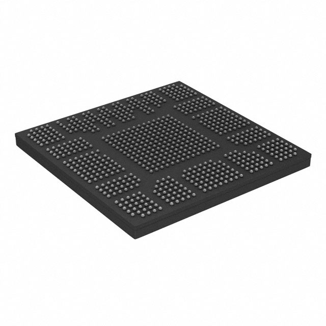
Package
The LFE5U-85F-7BG756I comes in a compact package, which ensures easy integration into electronic systems. The package provides protection against environmental factors and facilitates efficient heat dissipation.
Essence
The essence of the LFE5U-85F-7BG756I lies in its ability to provide a customizable and high-performance hardware platform for implementing complex digital logic circuits.
Packaging/Quantity
Each package of LFE5U-85F-7BG756I contains one unit of the FPGA.
Specifications
- Model: LFE5U-85F-7BG756I
- Technology: Field Programmable Gate Array (FPGA)
- Logic Elements: 85,000
- Package Type: BG756
- Operating Voltage: 1.2V
- Maximum Operating Frequency: 500 MHz
- I/O Pins: 756
- Memory Blocks: 4,800 Kbits
- Embedded Multipliers: 96
- DSP Blocks: 120
Detailed Pin Configuration
The LFE5U-85F-7BG756I has a total of 756 I/O pins, each serving a specific purpose in the circuit design. The pin configuration is detailed in the product datasheet, which provides information on the functionality and connectivity of each pin.
Functional Features
- High-performance digital logic processing
- Configurable I/O interfaces
- Embedded memory blocks for data storage
- Support for complex mathematical operations with embedded multipliers and DSP blocks
- Flexible clock management and synchronization capabilities
- On-chip programming and configuration options
Advantages and Disadvantages
Advantages
- Customizable hardware platform for specific applications
- High-performance data processing capabilities
- Low power consumption compared to traditional ASIC designs
- Reprogrammable design allows for iterative development and updates
- Wide range of I/O interfaces for versatile connectivity options
Disadvantages
- Higher cost compared to off-the-shelf integrated circuits
- Limited resources and capacity compared to application-specific designs
- Steeper learning curve for programming and configuring the FPGA
Working Principles
The LFE5U-85F-7BG756I operates based on the principles of field-programmable gate arrays. It consists of a matrix of configurable logic elements interconnected through programmable routing channels. The user can program the FPGA using a Hardware Description Language (HDL) to define the desired digital logic circuitry. Once programmed, the FPGA executes the specified logic functions, providing high-speed data processing capabilities.
Detailed Application Field Plans
The LFE5U-85F-7BG756I finds applications in various fields, including:
- Communications: Used in wireless communication systems, network routers, and base stations for signal processing and protocol implementation.
- Industrial Automation: Employed in control systems, robotics, and machine vision applications for real-time data processing and control algorithms.
- Aerospace and Defense: Utilized in radar systems, avionics, and military equipment for high-speed signal processing and encryption.
- Medical Devices: Integrated into medical imaging systems, patient monitoring devices, and diagnostic equipment for data processing and analysis.
- Automotive: Used in advanced driver assistance systems (ADAS), infotainment systems, and engine control units for real-time processing and control.
Detailed and Complete Alternative Models
- LFE5U-45F-7BG756I: A lower-capacity version of the LFE5U series FPGA with 45,000 logic elements.
- LFE5U-115F-7BG756I: A higher-capacity version of the LFE5U series FPGA with 115,000 logic elements.
- LFE5U-25F-7BG756I: A lower-cost version of the LFE5U series FPGA with 25,000 logic elements.
These alternative models provide different capacity options to suit specific application requirements.
In conclusion, the LFE5U-85F-7BG756I is a high-performance FPGA that offers flexibility, reprogrammability, and advanced features. It finds applications in various fields, providing customizable hardware platforms for implementing complex digital logic circuits.
기술 솔루션에 LFE5U-85F-7BG756I 적용과 관련된 10가지 일반적인 질문과 답변을 나열하세요.
Sure! Here are 10 common questions and answers related to the application of LFE5U-85F-7BG756I in technical solutions:
Q: What is the LFE5U-85F-7BG756I? A: The LFE5U-85F-7BG756I is a field-programmable gate array (FPGA) manufactured by Lattice Semiconductor.
Q: What are the key features of the LFE5U-85F-7BG756I? A: The key features include 85,000 logic cells, 756 I/O pins, high-speed transceivers, embedded memory blocks, and support for various communication protocols.
Q: What are some typical applications of the LFE5U-85F-7BG756I? A: The LFE5U-85F-7BG756I is commonly used in applications such as telecommunications, industrial automation, video processing, aerospace, and defense.
Q: How can I program the LFE5U-85F-7BG756I? A: The LFE5U-85F-7BG756I can be programmed using hardware description languages (HDLs) like VHDL or Verilog, or through graphical programming tools provided by Lattice Semiconductor.
Q: What is the power supply requirement for the LFE5U-85F-7BG756I? A: The LFE5U-85F-7BG756I requires a voltage supply of 1.2V for core logic and 3.3V for I/O banks.
Q: Can I interface the LFE5U-85F-7BG756I with other components or devices? A: Yes, the LFE5U-85F-7BG756I supports various communication protocols like UART, SPI, I2C, PCIe, Ethernet, and more, allowing easy interfacing with other components or devices.
Q: Does the LFE5U-85F-7BG756I have built-in memory? A: Yes, the LFE5U-85F-7BG756I has embedded memory blocks that can be used for storing data or implementing memory-intensive functions.
Q: Can the LFE5U-85F-7BG756I handle high-speed data transmission? A: Yes, the LFE5U-85F-7BG756I is equipped with high-speed transceivers that support protocols like Gigabit Ethernet, PCI Express, and Serial RapidIO.
Q: Is the LFE5U-85F-7BG756I suitable for real-time signal processing applications? A: Yes, the LFE5U-85F-7BG756I's high logic capacity and fast performance make it well-suited for real-time signal processing tasks such as image or video processing.
Q: Where can I find additional resources and support for working with the LFE5U-85F-7BG756I? A: Lattice Semiconductor provides comprehensive documentation, application notes, reference designs, and technical support on their website to assist users in working with the LFE5U-85F-7BG756I.