

LFXP2-30E-5FTN256I
Product Overview
Category
LFXP2-30E-5FTN256I belongs to the category of Field-Programmable Gate Arrays (FPGAs).
Use
This product is primarily used in digital logic circuits for various applications such as telecommunications, automotive, industrial automation, and consumer electronics.
Characteristics
- High-performance FPGA with advanced features
- Low power consumption
- Flexible and reconfigurable design
- Large number of programmable logic elements
- High-speed interfaces for data transfer
- Support for various communication protocols
Package
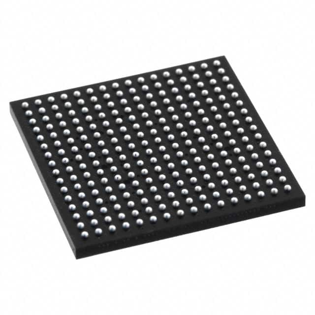
LFXP2-30E-5FTN256I comes in a compact and durable package suitable for surface mount technology (SMT) assembly. The package ensures protection against environmental factors and facilitates easy integration into electronic systems.
Essence
The essence of LFXP2-30E-5FTN256I lies in its ability to provide a customizable and adaptable solution for complex digital circuit designs. It allows designers to implement their desired functionality by programming the FPGA, eliminating the need for custom hardware development.
Packaging/Quantity
LFXP2-30E-5FTN256I is typically packaged in reels or trays, depending on the manufacturer's specifications. The quantity per package may vary, but it is commonly available in quantities suitable for both prototyping and production purposes.
Specifications
- Logic Elements: 30,000
- Block RAM: 1,080 Kbits
- DSP Slices: 96
- I/O Pins: 256
- Operating Voltage: 1.2V
- Maximum Frequency: 400 MHz
- Configuration Memory: Flash-based
Detailed Pin Configuration
For a detailed pin configuration diagram of LFXP2-30E-5FTN256I, please refer to the product datasheet provided by the manufacturer.
Functional Features
- High-speed data processing and manipulation
- Support for various communication protocols (e.g., Ethernet, USB, SPI)
- On-chip memory resources for efficient data storage and retrieval
- Flexible I/O capabilities for interfacing with external devices
- Reconfigurable architecture allows for dynamic changes in functionality
- Built-in security features to protect sensitive information
Advantages and Disadvantages
Advantages
- Flexibility: LFXP2-30E-5FTN256I offers a high degree of flexibility, allowing designers to adapt their designs to changing requirements.
- Time-to-Market: By utilizing FPGAs, developers can significantly reduce the time required for hardware development, accelerating the overall product development cycle.
- Cost-Effective: FPGAs eliminate the need for custom ASICs, reducing development costs and enabling cost-effective solutions for low to medium volume applications.
- Performance: With its high-speed interfaces and large number of logic elements, LFXP2-30E-5FTN256I provides excellent performance for demanding applications.
Disadvantages
- Power Consumption: FPGAs tend to consume more power compared to dedicated application-specific integrated circuits (ASICs).
- Complexity: Designing and programming FPGAs require specialized knowledge and expertise, making it more challenging for novice users.
- Limited Resources: Despite their flexibility, FPGAs have finite resources, which may restrict the complexity and scale of designs.
Working Principles
LFXP2-30E-5FTN256I operates based on the principles of reconfigurable computing. It consists of an array of programmable logic elements interconnected through configurable routing resources. The device's behavior is determined by the configuration data stored in its flash-based memory. During operation, the FPGA can be dynamically reprogrammed to implement different logic functions, enabling rapid prototyping and design iterations.
Detailed Application Field Plans
LFXP2-30E-5FTN256I finds applications in various fields, including:
- Telecommunications: Used in base stations, network switches, and routers for high-speed data processing and protocol handling.
- Automotive: Employed in advanced driver-assistance systems (ADAS), infotainment systems, and engine control units (ECUs) for real-time data processing and control.
- Industrial Automation: Utilized in programmable logic controllers (PLCs), motor control systems, and robotics for precise control and automation tasks.
- Consumer Electronics: Integrated into smart TVs, gaming consoles, and wearable devices to enable complex functionality and connectivity.
Detailed and Complete Alternative Models
- Xilinx Artix-7 XC7A35T-1CPG236C
- Intel Cyclone V EP5CE115F23C8N
- Microsemi SmartFusion2 M2S010S-1FGG484I
- Lattice ECP5-12K-5FN256C
These alternative models offer similar capabilities and can be
기술 솔루션에 LFXP2-30E-5FTN256I 적용과 관련된 10가지 일반적인 질문과 답변을 나열하세요.
Sure! Here are 10 common questions and answers related to the application of LFXP2-30E-5FTN256I in technical solutions:
Q: What is the LFXP2-30E-5FTN256I? A: The LFXP2-30E-5FTN256I is a field-programmable gate array (FPGA) manufactured by Lattice Semiconductor.
Q: What are the key features of the LFXP2-30E-5FTN256I? A: The key features include 30,000 logic elements, 256-pin package, low power consumption, and high-speed performance.
Q: What are some typical applications of the LFXP2-30E-5FTN256I? A: The LFXP2-30E-5FTN256I is commonly used in industrial automation, telecommunications, automotive electronics, medical devices, and aerospace applications.
Q: How can I program the LFXP2-30E-5FTN256I? A: The LFXP2-30E-5FTN256I can be programmed using various development tools such as Lattice Diamond, iCEcube2, or third-party programming tools compatible with Lattice FPGAs.
Q: What is the power supply requirement for the LFXP2-30E-5FTN256I? A: The LFXP2-30E-5FTN256I requires a single power supply voltage of 1.2V.
Q: Can I interface the LFXP2-30E-5FTN256I with other components or devices? A: Yes, the LFXP2-30E-5FTN256I supports various standard interfaces such as SPI, I2C, UART, and GPIOs, allowing easy integration with other components or devices.
Q: What is the maximum operating frequency of the LFXP2-30E-5FTN256I? A: The LFXP2-30E-5FTN256I can operate at a maximum frequency of up to 400 MHz.
Q: Can I use the LFXP2-30E-5FTN256I for real-time signal processing applications? A: Yes, the LFXP2-30E-5FTN256I's high-speed performance makes it suitable for real-time signal processing applications.
Q: Does the LFXP2-30E-5FTN256I support secure boot or encryption features? A: Yes, the LFXP2-30E-5FTN256I provides built-in security features such as bitstream encryption and authentication to protect your designs.
Q: Where can I find additional technical documentation and support for the LFXP2-30E-5FTN256I? A: You can find datasheets, application notes, reference designs, and technical support on the official website of Lattice Semiconductor or by contacting their customer support team.