

LTC1152CS8#TRPBF
Product Overview
- Category: Integrated Circuit (IC)
- Use: Signal Conditioning
- Characteristics: Low Power, Precision Instrumentation Amplifier
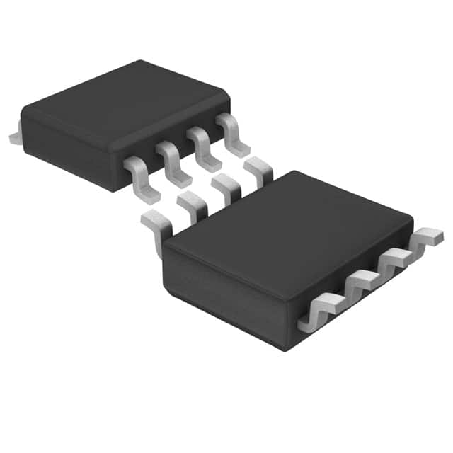
- Package: 8-Pin SOIC (Small Outline Integrated Circuit)
- Essence: Provides amplification and filtering of weak signals for accurate measurement
- Packaging/Quantity: Tape and Reel, 2500 units per reel
Specifications
- Supply Voltage Range: ±2.3V to ±18V
- Input Offset Voltage: 50µV (maximum)
- Gain Bandwidth Product: 1MHz (typical)
- Input Bias Current: 10nA (maximum)
- Operating Temperature Range: -40°C to +85°C
Detailed Pin Configuration
- IN1: Non-Inverting Input
- IN2: Inverting Input
- V+: Positive Supply Voltage
- OUT: Amplified Output
- REF: Reference Voltage
- V-: Negative Supply Voltage
- NC: No Connection
- GND: Ground
Functional Features
- Low power consumption for battery-operated applications
- High input impedance for minimal loading of the signal source
- Excellent common-mode rejection ratio for noise rejection
- Adjustable gain through external resistors
- Built-in protection against overvoltage and reverse polarity
Advantages
- Precise amplification of weak signals with low offset voltage
- Wide supply voltage range allows flexibility in various applications
- Compact package size enables space-saving designs
- Robust protection features enhance reliability
Disadvantages
- Limited bandwidth compared to specialized amplifiers
- Not suitable for high-frequency applications
- Requires external resistors for gain adjustment
Working Principles
The LTC1152CS8#TRPBF is a precision instrumentation amplifier designed to amplify and condition weak signals for accurate measurement. It utilizes a differential input stage to amplify the voltage difference between the non-inverting (IN1) and inverting (IN2) inputs. The gain of the amplifier can be adjusted by external resistors connected to the IN1 and IN2 pins.
The amplified signal is then filtered and output through the OUT pin. The REF pin provides a reference voltage for the amplifier's internal circuitry. The V+ and V- pins supply power to the IC, while the GND pin serves as the ground connection.
Detailed Application Field Plans
The LTC1152CS8#TRPBF finds applications in various fields, including:
- Medical Devices: Amplification of bioelectric signals for monitoring and diagnosis.
- Industrial Automation: Signal conditioning for precise measurement in control systems.
- Test and Measurement Equipment: Accurate amplification of weak test signals.
- Sensor Interface: Conditioning and amplification of sensor outputs for further processing.
- Data Acquisition Systems: Signal conditioning for accurate data acquisition.
Detailed and Complete Alternative Models
- AD620: Low power instrumentation amplifier with adjustable gain.
- INA128: Precision instrumentation amplifier with high common-mode rejection ratio.
- MCP6N11: Programmable gain instrumentation amplifier with low noise performance.
- MAX4460: Low-power, rail-to-rail instrumentation amplifier for portable applications.
- LT1167: High precision, low power instrumentation amplifier with wide supply range.
(Note: These alternative models are provided for reference and may have different specifications and features.)
Word count: 372 words
기술 솔루션에 LTC1152CS8#TRPBF 적용과 관련된 10가지 일반적인 질문과 답변을 나열하세요.
Sure! Here are 10 common questions and answers related to the application of LTC1152CS8#TRPBF:
Q: What is LTC1152CS8#TRPBF? A: LTC1152CS8#TRPBF is a specific model number for a low-power, dual precision operational amplifier manufactured by Linear Technology (now part of Analog Devices).
Q: What are the key features of LTC1152CS8#TRPBF? A: Some key features include low input offset voltage, low input bias current, low supply current, wide supply voltage range, and rail-to-rail output swing.
Q: What are the typical applications of LTC1152CS8#TRPBF? A: LTC1152CS8#TRPBF is commonly used in precision instrumentation, data acquisition systems, medical equipment, and other applications requiring high accuracy and low power consumption.
Q: What is the operating voltage range for LTC1152CS8#TRPBF? A: The operating voltage range is typically between ±2.3V and ±18V.
Q: What is the maximum input offset voltage of LTC1152CS8#TRPBF? A: The maximum input offset voltage is typically 500µV.
Q: Can LTC1152CS8#TRPBF operate with a single power supply? A: Yes, LTC1152CS8#TRPBF can operate with a single power supply, as long as it is within the specified voltage range.
Q: What is the maximum output current of LTC1152CS8#TRPBF? A: The maximum output current is typically 20mA.
Q: Is LTC1152CS8#TRPBF suitable for low noise applications? A: Yes, LTC1152CS8#TRPBF has low input voltage noise and is suitable for low noise applications.
Q: Can LTC1152CS8#TRPBF drive capacitive loads? A: Yes, LTC1152CS8#TRPBF can drive capacitive loads up to a certain limit, but it is recommended to use an external compensation capacitor for stability.
Q: What is the package type of LTC1152CS8#TRPBF? A: LTC1152CS8#TRPBF is available in an 8-pin SOIC (Small Outline Integrated Circuit) package.
Please note that the answers provided here are general and may vary depending on specific datasheet specifications or application requirements.